




To make a double sided PCB, you need copper patterns on both the top and bottom layers, accurate layer alignment, drilled holes, and reliable plated through holes or other interlayer connections. A simple hobby board may use wire jumpers or rivets, but a production double sided PCB should use plated vias, controlled registration, solder mask, surface finish, inspection, and electrical testing.
This guide explains the practical workflow, where DIY methods usually fail, and what to prepare when sending a double sided PCB design for manufacturing review.
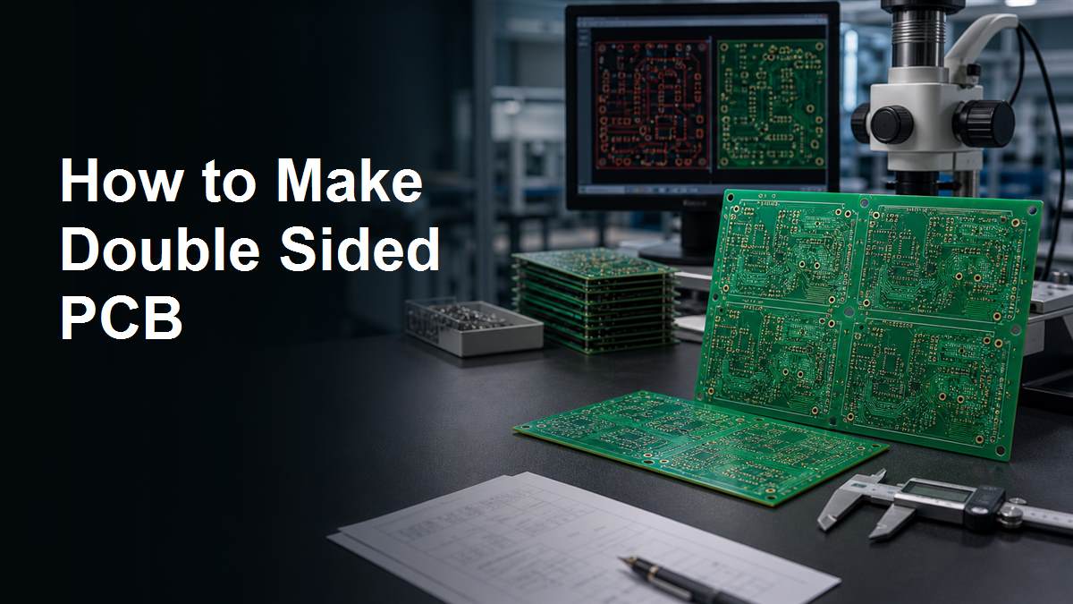
Understand What Makes a PCB Double Sided
A double sided PCB has copper on both sides of the insulating laminate. The top layer and bottom layer can both carry traces, pads, planes, and component connections. The two layers are connected through vias, plated holes, component leads, or designed interconnect points.
This is different from a single sided PCB where almost all copper routing is on one side. Double sided routing gives more space, better grounding options, and cleaner layouts, but it also adds alignment, drilling, plating, and inspection requirements. For basic board terminology, this PCB design overview is a useful background reference.
Start With a Layout That Uses Both Layers on Purpose
A double sided PCB should not use the second layer only because the first layer became crowded. Decide what each layer should do. One common approach is to route signals on both sides while keeping ground copper as continuous as possible.
Before exporting files, review component placement, trace width, clearance, return paths, drill sizes, and via count. If the design has dense routing or fast signals, read through practical PCB layout considerations before the design is frozen.
Choose How the Two Copper Layers Will Connect
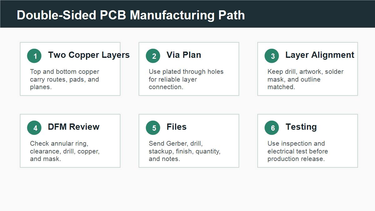
The most important manufacturing difference is the layer connection method. In professional PCB production, plated through holes connect the top and bottom copper. The hole wall is metallized, so current can pass between layers reliably.
DIY methods sometimes use wire jumpers, eyelets, or soldered component leads to connect layers. Those can work for experiments, but they are less reliable for repeatable production. If the board will be assembled, tested, shipped, or used in a product, specify plated through holes and let the manufacturer review drill and annular ring limits.
Control Layer Alignment, Drill Registration, and Board Outline
Double sided PCB manufacturing depends on registration. The top copper, bottom copper, drill file, solder mask, silkscreen, and board outline must line up. If they do not, pads may be off-center, holes may break out of annular rings, and solder mask openings may expose the wrong copper.
For a manufacturer, this means your output files must include the correct board outline, drill data, copper layers, solder mask layers, silkscreen layers, and any slots or cutouts. For a DIY process, it means the transfer or exposure must be aligned very carefully on both sides before etching.
Compare DIY Double Sided PCB and Factory Manufacturing
DIY double sided PCBs are useful for learning, quick experiments, or very simple circuits. Factory manufacturing is better when the board needs plated vias, solder mask, controlled drilling, fine clearances, repeatability, assembly, or electrical testing.
| Decision Point | DIY Method | Factory Manufacturing |
| Layer connection | Jumpers, rivets, component leads | Plated through holes and vias |
| Alignment | Manual transfer or exposure | Controlled registration process |
| Solder mask | Often missing or manual | Applied as standard production layer |
| Repeatability | Good for experiments | Better for prototypes and production |
| Testing | Manual continuity checks | Inspection and electrical test options |
Check Via Size, Annular Ring, and Drill Limits
Vias are small but they decide whether a double sided PCB works reliably. A via needs a drill hole, plated barrel, pad diameter, and annular ring. If the pad is too small for the drill tolerance, the hole can break out and weaken the layer connection.
Use manufacturer limits for minimum drill, finished hole size, annular ring, via diameter, and spacing. For more complex layer interconnects, the article on blind and buried vias in PCBs helps separate normal plated through holes from advanced via structures.
Run DFM Checks Before Sending the Files
DFM checks whether the double sided PCB can be manufactured within process limits. Check trace width, clearance, drill size, annular ring, solder mask slivers, copper-to-edge clearance, silkscreen over pads, board outline, and panel requirements.
A clean layout-rule check in software is helpful, but it is not the same as manufacturing review. DFM also checks whether the design is practical for drilling, plating, solder mask, inspection, and assembly. This is why DFM and DFA in PCB manufacturing should be part of the file handoff.
Prepare Gerber, Drill, Stackup, and Finish Details
A manufacturer needs complete files to make a double sided PCB. Send top copper, bottom copper, solder mask, silkscreen, board outline, NC drill, drill map if available, stackup notes, copper weight, board thickness, surface finish, quantity, and any impedance or testing requirements.
If assembly is needed, also send BOM, CPL, assembly drawing, polarity notes, and test requirements. Do not assume the manufacturer can infer missing details from screenshots or layout software files alone.
Double Sided PCB Checklist Before Manufacturing
Use this checklist before releasing a double sided PCB design.
- Top and bottom copper layers are exported correctly.
- Vias and plated holes use manufacturable drill and pad sizes.
- Drill file matches the board outline and copper pads.
- Annular rings are large enough for production tolerance.
- Solder mask openings do not create slivers or expose unwanted copper.
- Silkscreen does not cover solderable pads.
- Ground return paths are reviewed, not only visible traces.
- Gerber, drill, stackup, finish, thickness, copper weight, and quantity are included.
- DFM review is requested before production if the board is new or dense.
FAQs About How to Make Double Sided PCB
Can I make a double sided PCB at home?
Yes, for simple experiments. However, home methods usually struggle with plated through holes, accurate alignment, solder mask, repeatability, and reliable inspection.
What connects the two sides of a double sided PCB?
Professional boards usually use plated through holes or vias. DIY boards may use jumpers, rivets, or component leads, but those methods are less consistent.
Do double sided PCBs need plated through holes?
For reliable production, yes. Plated through holes create a controlled electrical connection between top and bottom copper layers.
What files are needed for a double sided PCB?
Send top and bottom copper Gerbers, solder mask, silkscreen, board outline, NC drill files, stackup notes, copper weight, finish, thickness, quantity, and special requirements.
Is a double sided PCB better than a single sided PCB?
It is better when the circuit needs more routing space, better grounding, smaller size, or cleaner placement. A simple circuit may still work well on a single sided PCB.
What is the biggest risk in double sided PCB design?
Common risks include poor via design, weak annular rings, layer misalignment, bad return paths, missing drill files, and unclear manufacturing notes.
Can PCBTRY review a double sided PCB before production?
Yes. Send Gerbers, drill files, stackup notes, copper weight, board thickness, finish, quantity, and assembly files if needed to [email protected].
Do I need solder mask for a double sided PCB?
For production boards, solder mask is strongly recommended. It helps prevent bridges, protects copper, improves assembly, and makes inspection cleaner.
How do I reduce cost on a double sided PCB?
Keep drill sizes reasonable, avoid unnecessary tight clearances, use standard thickness and finish when possible, and send complete files so quotation is not delayed.
Send Double Sided PCB Files for DFM Review
If your double sided PCB design is ready, send Gerber files, NC drill files, board outline, stackup notes, copper weight, surface finish, board thickness, quantity, and any BOM/CPL files to [email protected]. PCBTRY can review via reliability, manufacturability, file completeness, and quote details before production.



0 Comments