




To make vias on a PCB, the manufacturer drills the via holes, cleans the hole walls, plates copper through the holes, then inspects hole size, plating quality, annular ring, and electrical continuity. In PCB design, you do not “paint” a via onto the finished board. You define via size, pad size, type, layer connection, and manufacturing notes in the PCB files, then the factory builds the vias during fabrication.
This guide explains how PCB vias are made in real manufacturing, what a designer should specify, and why home-made wire jumpers are not the same as factory plated through holes.
Start With What a PCB Via Does
A via is a small plated hole that connects copper from one PCB layer to another. On a simple 2 layer board, a via usually connects the top copper to the bottom copper. On multilayer boards, vias may connect outer layers, inner layers, or selected layers only.
The important point is that a via is both an electrical connection and a manufacturing feature. If the hole is too small, the annular ring is too narrow, or the plating is weak, the via can become a reliability risk instead of a clean connection.
How a Factory Makes Plated Through Vias
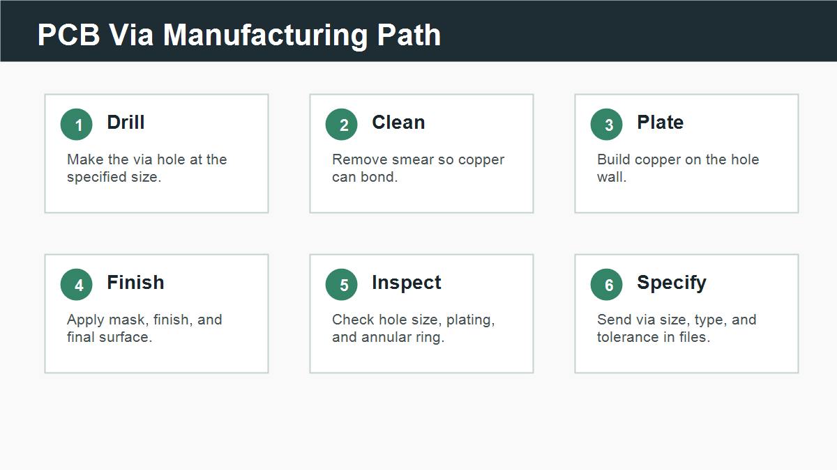
Factory vias are normally made before solder mask and final finish. The board panel is drilled, cleaned, chemically prepared, copper plated, patterned, etched, and inspected. The copper barrel on the hole wall is what carries the connection through the board.
Step 1: drill the hole at the specified finished size plus process allowance.
Step 2: clean resin smear and prepare the hole wall so copper can bond.
Step 3: deposit and electroplate copper through the hole.
Step 4: complete imaging, etching, solder mask, surface finish, routing, and testing.
Why DIY Wire Vias Are Not the Same as Factory Vias
For a home prototype, some people pass a wire through a hole and solder both sides. That can connect two copper sides, but it is not the same as a plated through hole. A factory via has a controlled copper barrel bonded to the hole wall, and it is made across the whole panel before final finishing.
Wire jumpers may work for a rough test, but they are not suitable for production reliability, dense layouts, impedance control, buried layers, or automated assembly. If the board needs repeatable manufacturing, specify real vias in the design files.
Choose the Right Via Type Before Layout
The via type depends on which layers need to connect. Through vias are common and economical. Blind vias connect an outer layer to an inner layer. Buried vias connect internal layers only. Microvias are used in HDI designs when routing density is high.
| Via Type | What It Connects | Typical Use |
| Through via | Top to bottom through the board | Most standard 2 layer and multilayer boards |
| Blind via | Outer layer to one or more inner layers | Dense routing and HDI designs |
| Buried via | Inner layers only | Advanced multilayer stackups |
| Microvia | Short laser-drilled layer connection | Fine-pitch BGA and compact HDI boards |
For deeper via type decisions, review PCBTRY’s guide to blind and buried vias in PCBs.
Specify Via Size, Pad Size, and Annular Ring
A via is not defined by hole size alone. You also need the pad diameter, finished hole size, copper thickness, clearance, aspect ratio, and annular ring. The annular ring is the copper pad area around the drilled hole. If the ring is too small, normal drilling tolerance can create breakout risk.
Do not guess very small via sizes just to make routing easier. Smaller vias may increase cost or require tighter process control. For production quotes, tell the manufacturer the minimum finished hole, minimum pad size, board thickness, copper weight, and layer count.
Check Aspect Ratio and Board Thickness
Aspect ratio compares board thickness with drilled hole size. A thick board with very small vias is harder to plate reliably. When the aspect ratio is too aggressive, copper may not plate evenly through the hole barrel.
This is why via size must be reviewed together with board thickness and stackup. A via that looks fine in CAD may be difficult or expensive in fabrication. For multilayer or dense boards, PCBTRY’s HDI PCB design guide explains why stackup and via planning must be decided early.
Use DFM Checks Before Releasing Via Files
Before sending the PCB to fabrication, run DFM checks for minimum drill, annular ring, copper clearance, solder mask opening, via-to-pad spacing, and via plugging or tenting requirements. Also check whether vias under components might wick solder or create assembly problems.
For a broader manufacturing review, PCBTRY’s DFM and DFA in PCB manufacturing guide is the right reference point. Via decisions can affect both fabrication and assembly, so they should not be left as a last-minute layout detail.
Via File Checklist Before Quotation
Use this checklist before asking for a PCB quote.
- Gerber files include all copper layers and solder mask layers.
- Drill file clearly separates plated and non-plated holes.
- Minimum finished hole size and pad size are known.
- Board thickness, layer count, copper weight, and material are specified.
- Blind, buried, microvia, via-in-pad, tented, plugged, or filled vias are clearly marked.
- Annular ring, clearance, and aspect ratio are checked against the manufacturer capability.
- Vias under components are checked for solder wicking and assembly risk.
- Impedance or high-speed nets are reviewed with stackup and via structure together.
FAQs About Making PCB Vias
Can I make vias on a PCB at home?
You can make simple wire-through connections for a prototype, but they are not the same as factory plated through vias and are not suitable for production reliability.
How are plated through vias made?
They are drilled, cleaned, chemically prepared, copper plated through the hole wall, then finished and inspected during PCB fabrication.
What file tells the factory where vias go?
The PCB design output usually includes Gerber copper layers and drill files. The drill file identifies hole locations and whether holes are plated or non-plated.
What is the difference between a via and a through hole?
A via mainly connects PCB layers. A through hole may also mount a component lead, connector, or mechanical feature.
Do all vias need solder mask openings?
No. Many vias are tented or covered by solder mask. Vias used as test points or special connections may need openings.
Why do small vias cost more?
Small vias can require tighter drilling, plating, aspect ratio control, and inspection, especially on thicker or multilayer boards.
Can blind vias be made on any PCB?
No. Blind vias need the right stackup and process planning. They should be confirmed with the manufacturer before final layout.
Can PCBTRY review my via design?
Yes. Send Gerbers, drill files, stackup, board thickness, copper weight, via requirements, quantity, and impedance notes to [email protected] for DFM review.
What is the biggest via mistake before fabrication?
A common mistake is using a via size or annular ring that the factory cannot reliably manufacture at the chosen board thickness.
Send Via and Stackup Files for DFM Review
If your PCB uses small vias, blind vias, buried vias, via-in-pad, HDI routing, or tight annular rings, send Gerbers, drill files, stackup, board thickness, copper weight, impedance notes, quantity, and special via requirements to [email protected]. PCBTRY can review via manufacturability before production.



0 Comments