




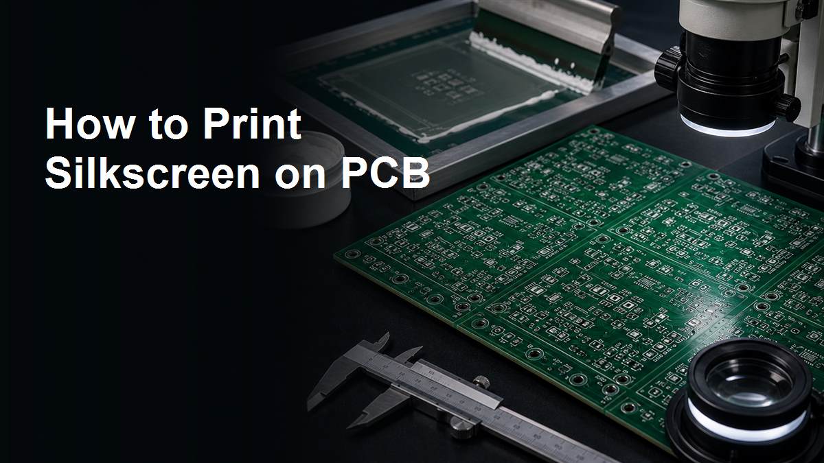
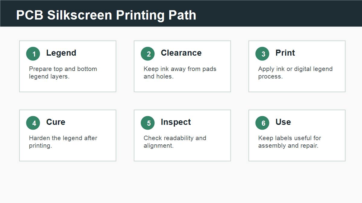
To print silkscreen on PCB, the designer first prepares top and bottom legend layers in the PCB files, keeps text and markings away from exposed pads and holes, then the manufacturer prints or applies the legend ink after solder mask and cures it before final inspection. Silkscreen is not an electrical copper layer. It is the printed information that helps assembly, testing, repair, and user identification.
This guide explains silkscreen in a beginner-friendly way: what the layer means, what should be printed, what should not be printed, and what to check before sending PCB files for fabrication.
Start With What PCB Silkscreen Means
PCB silkscreen is the printed legend on the board surface. It may show reference designators, polarity marks, connector labels, logos, pin numbers, warning marks, or assembly notes. It helps people know where parts go and how the board should be inspected.
A simple way to understand it is this: copper carries electricity, solder mask protects copper, and silkscreen teaches humans how to read the board. If you mix these layers up, the board can become hard to assemble or inspect.
Prepare the Top and Bottom Legend Layers
Silkscreen starts in the design file. Most PCB tools export top legend and bottom legend layers. These layers tell the factory what text and symbols should appear on each side of the board.
Step 1: decide what users, assemblers, and inspectors need to read. Step 2: place reference designators and polarity marks near the related parts. Step 3: export legend layers with Gerbers. Step 4: check the Gerber output, not only the CAD screen.
Keep Silkscreen Away From Pads and Holes
Silkscreen ink should not sit on solder pads, test pads, plated holes, connector contacts, or exposed copper areas. If ink lands on a solderable area, it can affect soldering, inspection, or electrical contact.
This is why manufacturers may clip or remove silkscreen that overlaps pads. If your text disappears after fabrication, it may be because the legend was placed too close to copper openings. For layout review basics, see PCBTRY’s guide on how to read PCB layout.
Choose Useful Marks Instead of Decorative Text
Good silkscreen saves time during assembly and repair. Prioritize reference designators, polarity marks, connector names, switch positions, test point labels, revision marks, and safety notes. Decorative text is less important than information that prevents wrong assembly.
For example, a diode polarity mark near D1 may prevent a reversed component. A connector pin 1 mark may prevent cable mistakes. A test point label may reduce debugging time.
Understand How the Factory Prints It
In production, the legend is applied after solder mask. Depending on the factory process, it may use screen printing, inkjet legend printing, or another controlled marking method. After printing, the legend is cured so it bonds to the board surface.
The exact process matters less to the buyer than the result: the text should be readable, aligned, durable enough for the application, and not printed where solder or contact is needed.
Check Size, Line Width, and Color Contrast
Silkscreen must be large enough to print and read. Very small text or thin lines may blur, break, or disappear. White legend on green solder mask is common because it gives strong contrast, but other solder mask colors may need extra care.
If the board is very dense, do not force every reference designator onto the board. It may be better to keep critical polarity and connector marks on the PCB and use an assembly drawing for the full reference list.
PCB Silkscreen Checklist Before Fabrication
- Top and bottom legend layers are included in the Gerber package.
- Reference designators are readable and near the correct parts.
- Polarity marks are clear for diodes, LEDs, capacitors, ICs, and connectors.
- Silkscreen does not overlap pads, holes, test points, or exposed copper.
- Text size and line width are within manufacturer capability.
- Connector labels and pin 1 marks are useful for assembly and testing.
- Dense areas use assembly drawings instead of unreadable tiny text.
- Final Gerber viewer check confirms what will actually be printed.
FAQs About Printing Silkscreen on PCB
Is PCB silkscreen the same as solder mask?
No. Solder mask is the protective coating over copper. Silkscreen is printed text or symbols on top of the board surface.
Can silkscreen be printed over solder pads?
It should not be. Manufacturers usually remove or clip silkscreen that overlaps pads or exposed copper.
What should be included in PCB silkscreen?
Use reference designators, polarity marks, connector labels, pin 1 marks, test point labels, revision marks, and safety notes when useful.
Why did my silkscreen disappear after fabrication?
It may have been too small, too thin, too close to pads, or clipped by manufacturing rules.
Can both sides of a PCB have silkscreen?
Yes, if the design includes top and bottom legend layers and the order specifies it.
What color is PCB silkscreen?
White is common, but other colors may be available depending on the manufacturer and solder mask color.
Does silkscreen affect PCB function?
It usually does not carry electricity, but wrong placement can interfere with soldering, contacts, or inspection.
What files tell the factory what to print?
The top and bottom legend Gerber layers define the silkscreen artwork.
Can PCBTRY review silkscreen before fabrication?
Yes. Send Gerbers, drill files, board color, silkscreen requirements, quantity, and any readability concerns to [email protected].
Send Silkscreen and Gerber Files for Review
If your PCB needs clear reference designators, polarity marks, connector labels, or special legend requirements, send Gerbers, drill files, board color, silkscreen color, quantity, and assembly notes to [email protected]. PCBTRY can review silkscreen manufacturability before production.



0 Comments