Blog
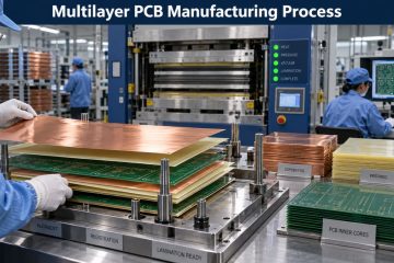
Multilayer PCB Manufacturing Process: Registration, Lamination and Testing
See how multilayer PCBs are fabricated from stack-up and inner layers through lamination, drilling, plating, inspection and electrical testing.



See how multilayer PCBs are fabricated from stack-up and inner layers through lamination, drilling, plating, inspection and electrical testing.
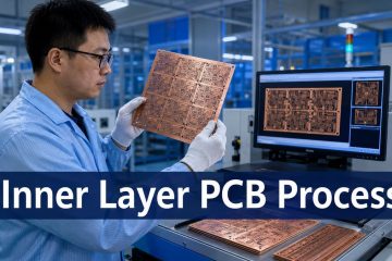
See how PCB inner layers move from CAM compensation and copper preparation through imaging, etching, AOI, oxide treatment, and lamination release checks.
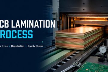
Learn how multilayer PCB lamination controls prepreg, resin flow, vacuum, temperature, pressure, registration, thickness, voids and delamination.
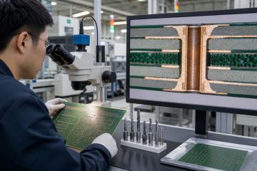
Learn how PCB vias are designed, drilled, desmeared and copper plated, how via treatments differ, and which DFM files and inspection checks prove quality.
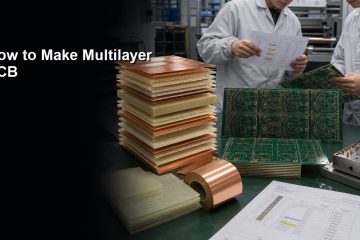
See how multilayer PCBs are designed, imaged, laminated, drilled, plated, finished, and tested, plus the files and DFM checks needed before fabrication.
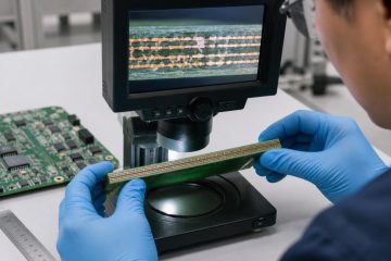
Learn how to identify PCB copper layers using design files, board-edge clues, vias, X-ray, and cross-section evidence, with clear limits for each method.
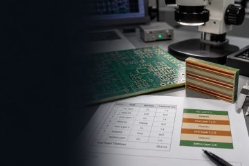
Learn a practical 4 layer PCB stackup, when to use signal-ground-power-signal layers, what to check for impedance, copper balance, vias and fabrication.
Learn how multilayer PCB boards are made, from stackup and inner layers to lamination, drilling, plating, testing and buyer DFM checks.
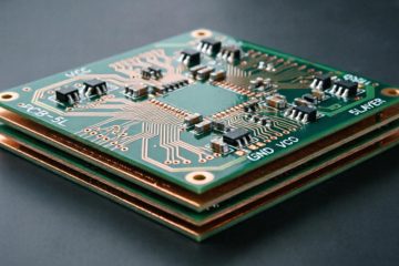
A multilayer PCB is used when a circuit needs more routing space, better signal control, higher component density, or stronger power distribution than a single-sided or double-sided board can provide. In real projects, multilayer boards are common in automotive electronics, industrial control, medical devices, communication equipment, servers, AI hardware, consumer Read more
If you have any enquiry about quotation or cooperation, please feel free to email us at [email protected] or use the following enquiry form. Oursales representative will contact you within 24 hours. Thank you for your interest in our products.