





The bare PCB manufacturing process transforms design files and copper-clad laminate into an unpopulated board with conductive traces, plated interconnections, solder mask, legend, surface finish, and a finished outline. It is used before component assembly and differs from PCBA production: bare-board fabrication builds the electrical and mechanical interconnect structure, while assembly later mounts and solders components.
For multilayer, impedance-controlled, fine-feature, or reliability-sensitive boards, the route must be planned around the actual stack-up, holes, materials, copper, finish, tolerances, and acceptance requirements. pcbtry supports CAM/DFM review, fabrication, inspection, and electrical testing. Send Gerber or ODB++ data, NC drill files, stack-up, fabrication drawing, quantity, and test requirements for an engineering review and quotation.
What Is a Bare PCB?
A bare PCB is a finished printed circuit board without assembled electronic components. It already contains the insulating structure, copper circuitry, pads, planes, vias, holes, solder mask, markings, surface finish, and routed profile specified by the fabrication data.
The term matters at quotation and inspection. Bare-board electrical test checks the manufactured connectivity against the released netlist; it does not prove that a populated product will boot, communicate, or meet its functional specification. Those later checks belong to PCBA inspection and functional test.
How Does the Bare PCB Manufacturing Process Work?
The exact route changes with layer count, via type, material, finish, and design rules, but conventional multilayer production follows one continuous sequence. Each step below states the output to control and the risk if that output drifts.
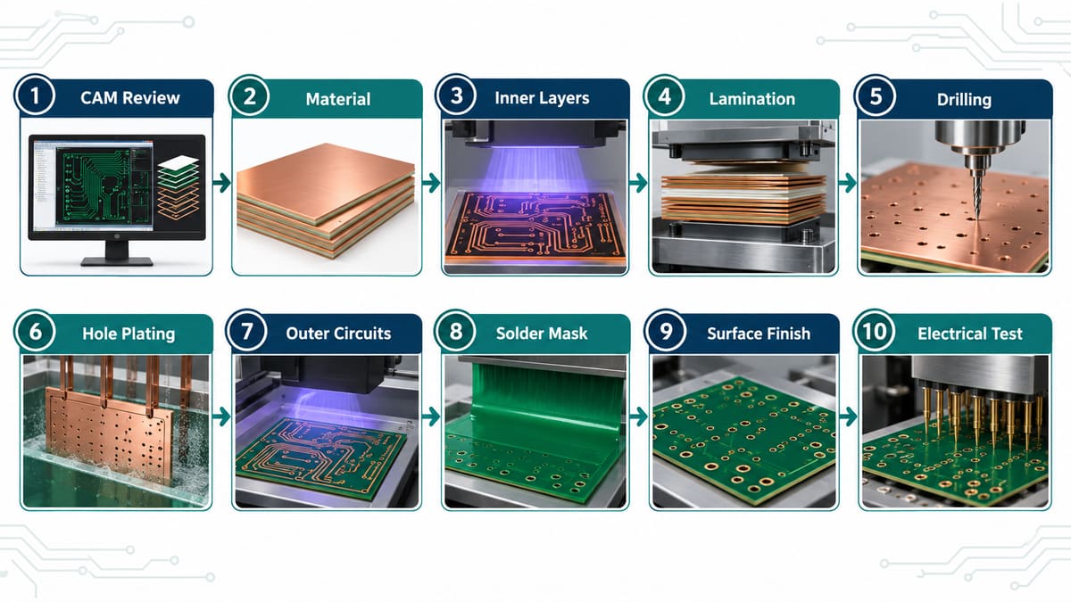
1. Engineering review and CAM preparation. The fabricator checks data completeness, layer order, drill-to-copper relationships, minimum features, panelization, impedance notes, materials, finish, outline, and tolerances. CAM generates controlled imaging, drilling, routing, inspection, and electrical-test data. A conflict between Gerber, drill, stack-up, and drawing must be resolved rather than guessed. See the practical role of PCB DFM review before production release.
2. Material preparation. Copper-clad cores and prepreg are selected by approved type, thickness, copper construction, and lot controls. Material is cut, identified, and conditioned as the process requires. A nominal material family is not a complete stack-up: resin system, glass style, copper, and finished thickness interact with impedance, drilling, lamination, and dimensional behavior. This FR-4 substrate explanation helps clarify what the material designation does—and does not—tell a buyer.
3. Inner-layer imaging, etching, and AOI. Photoresist is applied to the copper surface, exposed with the circuit image, developed, and etched so the required inner-layer copper remains. AOI compares the imaged circuitry with released data before it disappears inside the stack. Imaging or etching drift can create necking, opens, shorts, copper islands, or feature-width changes that later inspection cannot directly see.
4. Oxide treatment, lay-up, and lamination. Clean inner layers, prepreg, and copper foils are stacked in the released sequence and pressed under a qualified cycle. The process must produce bond integrity, controlled thickness, resin distribution, and layer registration. Excess or insufficient resin flow, contamination, incorrect lay-up, or registration movement can cause voids, delamination, thickness error, or drill breakout.
5. Drilling and hole-wall preparation. CNC tools create through-holes and mechanical holes; laser drilling or sequential build-up may be added for HDI structures. Tool condition, hit count, entry/backup material, panel support, and registration affect hole position and wall quality. Desmear and related preparation remove resin debris and condition the dielectric so metallization can bond. Poor preparation can leave an electrically intermittent hole even when its diameter appears correct.
6. Electroless copper and electrolytic plating. A conductive seed layer is deposited on nonconductive hole walls, then copper is built to the required construction. Current distribution, chemistry, agitation, panel loading, and contact condition influence thickness and uniformity. Thin or discontinuous hole-wall copper creates reliability risk; excessive or uneven surface copper can make later feature formation harder.
7. Outer-layer imaging, pattern plating, and etching. The outer circuit pattern is imaged, required features receive additional plating and an etch-resistant layer where the chosen route requires it, then unwanted copper is removed. The engineer watches line width/spacing, plating distribution, resist condition, and etch balance. A process that protects one feature may still over-etch another area if panel density and compensation are not controlled.
8. Solder mask and legend. The board is cleaned, coated with solder mask, imaged, developed, and cured; legend is then applied as specified. Registration, adhesion, cleanliness, cure, and dam geometry affect exposed pads and assembly yield. Mask encroachment can reduce the solderable area, while under-cure or contamination can create adhesion and cleanliness problems.
9. Surface finish. The selected finish protects exposed copper and provides the surface needed for assembly or contact. HASL, ENIG, OSP, immersion tin, immersion silver, hard gold, and other finishes have different flatness, storage, contact, process, and cost implications. The finish must match the component pitch, assembly process, end use, and drawing—not simply a habit from a previous design. For one example, review how immersion tin surface finish changes handling and selection.
10. Profiling, electrical test, final inspection, and packing. Routing, scoring, punching, or another approved method creates the outline and panel features. Electrical test checks opens and shorts against the released test data. Dimensional, visual, finish, marking, cleanliness, and specified coupon or microsection checks complete acceptance. Packing must protect the finish, board flatness, cleanliness, and traceability until assembly.
Which Inputs Control the Manufacturing Route?
Two boards with the same outline can require very different routes. The route is selected from the design package, not from the keyword “PCB.”
| Design input | Process decision it changes | Risk if unspecified or inconsistent |
|---|---|---|
| Layer count and stack-up | Core/prepreg construction, lay-up, lamination, impedance plan | Wrong thickness, dielectric spacing, or layer order |
| Hole table and via structure | Mechanical/laser drilling, sequential lamination, plating route | Unbuildable holes, breakout, weak interconnects |
| Minimum line/space and copper | Imaging, compensation, plating, and etching window | Opens, shorts, width loss, uncontrolled geometry |
| Material specification | Procurement, storage, lamination, drilling, reliability controls | Substitution or performance mismatch |
| Surface finish | Final finish chemistry and downstream handling | Flatness, solderability, contact, or shelf-life mismatch |
| Tolerances and acceptance class | Tooling, inspection, sampling, coupons, documentation | Quote ambiguity or rejected product after fabrication |
Where Do Bare PCB Defects Start?
Most defects can be traced to a requirement, material, imaging, lamination, drilling, metallization, finish, handling, or test-control failure. The detection point is not always the origin point.
| Failure | Origin, impact, and checkpoint |
|---|---|
| Open or short | Imaging, resist, etching, contamination, or test-data error can create wrong connectivity. Check the AOI stage, electrical-test method, and released netlist. |
| Hole-wall void or thin copper | Drill preparation, desmear, activation, or plating distribution can cause intermittent or life-cycle failure. Define the coupon/microsection plan and plating evidence. |
| Layer misregistration | Artwork scaling, lay-up, lamination movement, or drilling alignment can reduce annular ring or cause breakout. Review the registration method and cross-section results. |
| Delamination or voiding | Material condition, contamination, press cycle, or resin flow can create mechanical and electrical reliability risk. Review traceability, lamination control, and acceptance. |
| Mask or finish defect | Surface preparation, registration, cure, chemistry, or handling can affect assembly or storage. Confirm visual criteria, finish requirement, and packing condition. |
How Are Bare PCBs Inspected and Tested?
Inspection is distributed across the route because final inspection cannot reveal every hidden condition. Inner-layer AOI checks circuitry before lamination; dimensional and feature measurements control mechanical and image outputs; coupons and microsections can reveal internal construction; final electrical test checks continuity and isolation; visual inspection checks workmanship and finish against the agreed criteria.
- AOI: detects image differences and candidate opens/shorts, but findings still require disposition.
- Microsection: reveals layer, hole-wall, plating, and internal construction at the sampled coupon or location.
- Electrical test: verifies the tested net connectivity, not assembled product function or every reliability mechanism.
- Impedance coupon test: checks the agreed coupon structure when controlled impedance is specified; coupon correlation and acceptance must be defined.
- Dimensional and visual inspection: confirms outline, holes, markings, surface condition, and other drawing requirements.
How Does Design Affect Bare PCB Reliability?
Design determines how much process margin exists. Small annular rings, aggressive via aspect ratios, dense copper transitions, mismatched tolerances, poorly defined stack-ups, unsupported material callouts, and conflicting file revisions can narrow the manufacturing window. A DFM question is not automatically a request to weaken the design; it is a request to decide which requirement controls when two instructions cannot both be met.
Release one fabrication package with a revision identifier. Include copper layers, solder mask, legend, profile, drill/rout data, stack-up, fabrication drawing, impedance table where needed, material/finish notes, quantity, acceptance standard, and any coupon or report requirement.
How Long Does Bare PCB Manufacturing Take?
Lead time depends on the released route and queue, so it should be quoted for the actual design. A simple prototype may use a standard material and one lamination cycle; an HDI, rigid-flex, special-material, heavy-copper, controlled-depth, or special-finish design may require added procurement, repeated build-up, coupons, external processing, or extra inspection.
Ask the supplier to separate engineering-question closure, material availability, fabrication time, inspection/report time, and shipping. “Production days” measured before files are approved can create a false delivery expectation.
How Should You Choose a Bare PCB Manufacturer?
Choose a manufacturer that can explain the route, control points, evidence, and exception process for your design. Equipment lists and generic capability tables are only a starting point.
- Can the supplier identify conflicts between fabrication files and drawing notes before release?
- Is the proposed stack-up documented, including material and copper construction?
- Which features are at the supplier’s routine capability, and which need special review or qualification?
- How are drill tools, hole preparation, plating, registration, and finish controlled for this board?
- Which inspection, coupon, electrical-test, and traceability records are included in the quote?
- How are deviations, substitutions, rework, and process changes approved?
- What information must the buyer provide before the delivery commitment begins?
Frequently Asked Questions
Is a bare PCB the same as a blank copper board?
No. A blank copper-clad laminate has not yet received the circuit pattern, holes, plating, mask, finish, and profile. A bare PCB is fully fabricated but has no assembled components.
Does the bare PCB process include soldering components?
No. Component placement and soldering belong to PCB assembly. Fabrication ends with the completed unpopulated board and its agreed inspection and test records.
Are all multilayer boards laminated only once?
No. Conventional multilayers may use one primary lamination cycle, while blind/buried vias or HDI sequential build-up can require repeated imaging, lamination, drilling, metallization, and inspection stages.
Why is desmear needed after drilling?
Mechanical drilling can leave resin debris on exposed internal copper and hole walls. The approved hole-preparation process removes or conditions this material so subsequent metallization can form a reliable connection.
Does electrical test guarantee PCB reliability?
No. It checks connectivity under the defined test method. Material condition, hole-wall quality, layer construction, cleanliness, and life-cycle performance need appropriate process controls and any additional agreed evidence.
Which surface finish should I specify?
Choose from component pitch, assembly process, contact function, storage/handling, application restrictions, and cost. Ask the assembler and fabricator to review the same requirement.
What files are needed for a bare PCB quote?
Send Gerber or another accepted fabrication dataset, NC drill/rout files, stack-up, fabrication drawing, impedance requirements, material and finish, quantities, acceptance criteria, and requested reports.
Can the factory change material without asking?
The quotation and drawing should define the approved material or substitution rule. If electrical, thermal, mechanical, flammability, reliability, or certification properties matter, require review before substitution.
Request a Bare PCB Manufacturing Review
Before release, send pcbtry the revision-controlled Gerber or ODB++ package, NC drill files, stack-up, fabrication drawing, material and surface-finish requirements, impedance table, tolerances, quantities, acceptance standard, and test/report needs. The engineering team can identify open questions, confirm the proposed route, and prepare a fabrication quotation.



0 Comments