




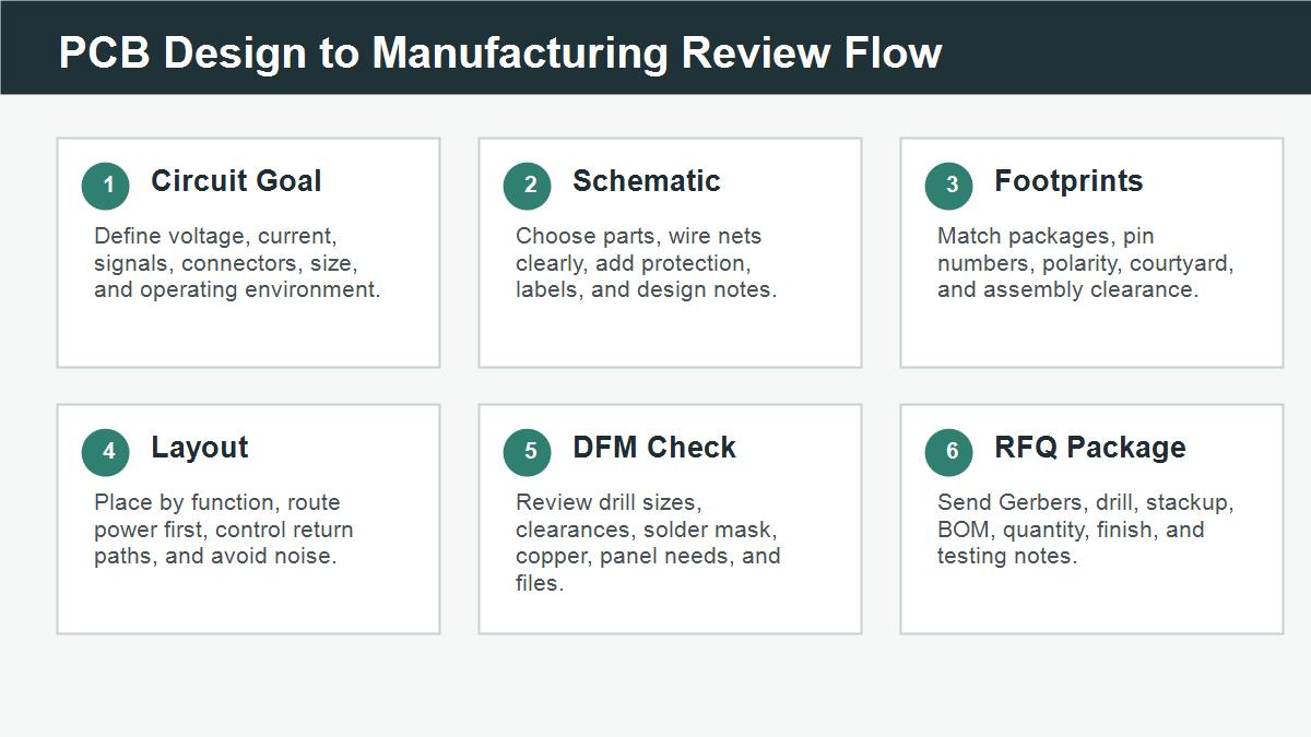
To design a PCB board for a circuit, start with a working schematic, choose footprints that match the real parts, place components by function, route power and ground first, separate noisy and sensitive signals, then run electrical and manufacturability checks before sending files for quotation. A PCB is the physical version of your circuit, so every schematic choice must survive fabrication, assembly, testing, and use.
This guide walks through the design path from circuit idea to quote-ready PCB files, with the checks that help a board move from layout software to real production.
Start With the Circuit Function Before the Board Shape
The first design decision is what the circuit must do, what power it needs, what signals it carries, where users or cables connect, and what environment it will face. These details control component choice, connector location, copper width, grounding, and test access.
Write the requirements in plain language before opening layout software: input voltage, output current, communication interfaces, sensor locations, mechanical size, thermal limits, and whether the board is a prototype or production design.
Create a Schematic That Can Be Reviewed
The schematic should show the electrical logic clearly enough that another engineer, manufacturer, or future version of you can review it. Use correct symbols, named nets, reference designators, power flags, decoupling capacitors, connector pin labels, and notes for special requirements.
A common mistake is drawing only enough to make the layout tool connect pins. If polarity, pullups, programming pins, reset lines, or connector pinouts are unclear in the schematic, the layout can look complete while the real board fails.
Choose Components and Footprints Together
Every selected component needs a matching footprint. Check the datasheet, package drawing, pin numbering, pad size, thermal pad, courtyard, and assembly orientation. Do not assume that two parts with the same package name use exactly the same footprint.
For PCB fabrication and assembly, footprint mistakes are expensive because they may not show until parts arrive or the first assembly is built. Confirm polarity marks for diodes, LEDs, electrolytic capacitors, IC pin one, connectors, and battery holders.
Decide Board Size, Mounting, Connectors, and Keep-Out Areas
The board outline should follow the product enclosure, mounting method, connector access, heat path, and assembly handling. Define screw holes, edge clearance, connector overhang, switch or LED locations, antenna keep-out zones, and areas that cannot contain copper or components.
If the PCB will be assembled by a manufacturer, also consider tooling strips, fiducials, panelization, and component clearance. A tiny board may save material cost but increase assembly and handling difficulty.
Place Components by Function, Heat, and Signal Flow
Good placement makes routing easier and reduces electrical problems. Group related parts together: power input and protection near the connector, regulator and capacitors close together, MCU support parts close to the IC, and high-current paths short and direct.
Think of current and signals as paths, not just wires. Sensitive analog or RF sections should not sit next to switching regulators, noisy motor drivers, or fast digital buses unless shielding, grounding, and routing are planned.
Route Power, Ground, and Return Paths First
Power and ground are the foundation of the board. Use copper widths that match current and temperature rise, keep high-current loops short, and give signals a clean return path. For two-layer boards, ground pours help, but they do not fix a broken return path.
If the circuit uses fast edges, switching power, RF, high current, or mixed analog and digital sections, the return path matters as much as the visible signal trace. Poor return paths can cause noise, EMI, unstable readings, and hard-to-debug failures.
Set Trace Width, Clearance, Drill, and Via Rules
Design rules should match both the circuit and the manufacturer. Set minimum trace width, spacing, via size, drill size, annular ring, solder mask expansion, copper-to-edge clearance, and preferred hole tolerances before routing the full board.
| Rule Area | What to Check | Why It Matters |
| Trace width | Current, heat, voltage drop | Prevents overheating and unstable power |
| Clearance | Voltage, fabrication limit, contamination risk | Reduces shorts and arcing risk |
| Via and drill | Manufacturer minimums and current path | Avoids drill breakout and weak connections |
| Solder mask | Pad openings and slivers | Controls solder bridges and assembly yield |
Use Planes, Pours, and Decoupling Correctly
Planes and copper pours help only when they are connected and placed with intent. A ground pour cut into islands by signal traces may not provide a useful return path. A power pour with thin necks may create voltage drop or heating.
Place decoupling capacitors close to the IC power pins, with short paths to ground. For regulators, follow datasheet layout guidance for input capacitors, output capacitors, feedback traces, and thermal copper.
Check High-Speed, Analog, RF, and High-Current Risks
Not every PCB needs controlled impedance, but every PCB needs risk separation. Fast digital signals, clocks, USB, RF paths, switching regulators, motor lines, battery current, and sensitive analog inputs should be routed with their behavior in mind.
If the board uses high-speed or RF signals, review stackup, trace geometry, reference planes, via transitions, connector launch, and return current. For high-current paths, review copper thickness, trace width, heat spreading, connector rating, and fuse or protection location.
Add Test Points, Labels, and Debug Access Early
Test access is easiest to add during layout and painful to add after fabrication. Add test points for power rails, ground, programming, reset, communication buses, key analog nodes, and important enable or fault signals.
Use clear silkscreen labels when space allows. If the board may go to assembly or production testing, ask the manufacturer what test point size, spacing, and side access are preferred before the design is frozen.
Run ERC, DRC, and Manual Review
Software checks catch many mistakes, but not all design mistakes. ERC can find unconnected pins or power flag issues. DRC can find clearance, drill, and mask problems. Manual review catches wrong connector direction, bad part orientation, thermal concerns, and missing manufacturing notes.
Do at least one review with the schematic and layout open side by side. Follow each connector, power rail, polarity-sensitive part, and critical signal from schematic to footprint to routed board.
Prepare Quote-Ready PCB Manufacturing Files
A manufacturer cannot quote or build accurately from screenshots. Prepare Gerber or ODB++ files, NC drill files, board outline, stackup notes, copper weight, material, surface finish, solder mask color, silkscreen color, quantity, and delivery target. For assembly, also prepare BOM, CPL, assembly drawing, and test requirements.
Common PCB Design Mistakes to Catch Before Ordering
The most common mistakes are wrong footprints, reversed polarity, missing mounting clearances, trace widths that do not match current, poor ground return, connectors facing the wrong direction, missing programming access, and incomplete manufacturing files.
Another common issue is routing a board that works electrically in software but is hard to build. Very small clearances, unusual drills, narrow copper necks, solder mask slivers, and unclear layer naming can all slow quotation or cause production questions.
Internal Links for Related Decisions
For related background, review what PCB design means, DFM and DFA in PCB manufacturing, FR4 substrate material, PCB copper thickness selection, and high speed PCB manufacturing support.
FAQs About Designing a PCB Board for a Circuit
Can a beginner design a PCB board for a simple circuit?
Yes. Start with a simple schematic, use verified footprints, keep the layout spacious, and run ERC, DRC, and manufacturer DFM checks before ordering.
What software can I use for PCB design?
Common choices include KiCad, EasyEDA, Altium Designer, Eagle/Fusion, OrCAD, and other EDA tools. The workflow is similar: schematic, footprints, board layout, checks, and export files.
Do I need a schematic before PCB layout?
Yes for most real boards. The schematic controls nets, part references, and review logic. Drawing copper directly is risky except for very simple experimental boards.
How do I know the correct trace width?
Base it on current, copper thickness, acceptable temperature rise, voltage drop, and manufacturer capability. High-current traces need wider copper or pours.
What files should I send for PCB fabrication?
Send Gerber or ODB++ files, NC drill files, board outline, stackup or material notes, copper weight, finish, solder mask, quantity, and any special requirements.
What files are needed for PCB assembly?
Assembly usually needs Gerbers, BOM, CPL or pick-and-place file, assembly drawing, polarity notes, quantity, and testing requirements.
Should I add test points to a prototype PCB?
Yes. Add test points for power rails, ground, programming, reset, key signals, and debug nodes. They save time during bring-up and production testing.
What is DFM in PCB design?
DFM means design for manufacturability. It checks whether the layout can be fabricated and assembled reliably within manufacturer limits.
Can PCBTRY review my PCB design before manufacturing?
Yes. Send Gerbers, stackup notes, BOM if assembly is needed, quantity, and special requirements to [email protected] for engineering review and quotation.
Send PCB Design Files for Manufacturing Review
If your circuit schematic is ready and you want a manufacturable PCB, send Gerber files, drill files, stackup notes, copper thickness, board quantity, surface finish, and any assembly BOM/CPL files to [email protected]. PCBTRY can review the files for DFM, fabrication risk, assembly needs, and quote details before production.



0 Comments