




What Does PCB Etch Factor Measure?
PCB etch factor measures how effectively copper is removed downward compared with how far the etchant attacks sideways under the resist. It is commonly expressed as vertical etch depth divided by lateral undercut on one side of a trace. A higher ratio means the trace sidewall is closer to vertical and the loss of top width is smaller.
The practical issue is not the ratio by itself. Etching changes the conductor that was drawn in CAD into a manufactured copper cross-section. That change can reduce finished trace width, tighten the remaining space, alter controlled impedance, and limit how reliably a fabricator can hold fine features.
Do not confuse etch factor with edge roughness. Edge roughness describes small irregularities along a conductor edge. Etch factor describes the relationship between downward copper removal and lateral undercut. Both can affect a fine or high-frequency trace, but they are different measurements.
Why Does Etching Create Undercut?
Undercut occurs because wet chemistry reaches exposed copper from more than one direction. While the etchant removes copper through its thickness, it also reaches sideways beneath the edge of the imaging resist. The protected conductor therefore does not retain a perfectly rectangular wall.
How much lateral attack occurs depends on the actual production process: starting copper, plated copper, chemistry, bath condition, temperature, spray pressure, conveyor speed, panel loading, copper distribution, and the time needed to clear unwanted copper. These are factory process variables, not values a designer can safely infer from a generic chart.
Outer layers and inner layers also do not always follow the same route. Outer-layer copper may include additional plated copper before final pattern etching, while an inner layer is commonly imaged and etched from its starting foil. The copper thickness that must be removed and the production compensation can therefore differ by layer.
How Do You Calculate Etch Factor and Width Loss?
The basic calculation uses EF = D / U, where D is the vertical copper depth removed and U is the lateral undercut on one side. Rearranging the equation gives U = D / EF. A simplified first-order width loss is twice the one-side undercut.
| Quantity | Meaning | Example |
| D | Copper depth removed | 35 µm |
| EF | Vertical depth divided by one-side undercut | 3.5 |
| U = D / EF | Estimated undercut on one side | 10 µm |
| 2U | Simplified total top-width loss | 20 µm |
In this teaching example, artwork that is 200 µm wide would have an estimated top width near 180 µm before any manufacturer compensation. It is an illustration, not a universal production allowance. Real traces have a process-dependent profile, copper may be plated, and the fabricator normally modifies working data so the finished conductor meets the released requirement.
The safest interpretation is: use the formula to understand sensitivity, not to rewrite production artwork using a guessed ratio.
What Does the Etched Trace Cross-Section Look Like?
An etched PCB trace is better modeled as a trapezoidal or slightly curved-sided conductor than as a perfect rectangle. The top, base, and sidewall profile depend on how the resist, copper thickness, plating, and etching process interact.
This distinction matters because different documents may use “trace width” without stating where it is measured. A CAD width, artwork width, top width, base width, and inspection result are not automatically identical. For a general circuit, the allowed finished-width tolerance may absorb the difference. For fine-line or controlled-impedance work, the measurement definition should be agreed with the fabricator.
If you need a foundation before reviewing cross-sections, see what a PCB trace is and what it carries.
How Does Copper Weight Change Etch Risk?
Thicker copper usually requires more process allowance because more copper must be removed before the open area clears. More etching time can increase absolute lateral undercut, so a trace-and-space combination that is comfortable on thin copper may be difficult on heavy copper.
| Design condition | Etch concern | What to verify |
| Thin copper with moderate features | Usually a wider process window | Finished trace/space and standard tolerance |
| Thick copper with narrow spaces | Longer removal and more undercut risk | Minimum space after CAM compensation |
| Outer layer with plated copper | Final copper may exceed starting foil | Finished copper target and outer-layer capability |
| Mixed copper weights by layer | Different layers may need different working data | Layer-specific stackup and finished copper table |
Avoid copying a minimum trace/space value from a standard 1 oz capability table into a 2 oz or 3 oz design. The same nominal feature can move from routine to special process when copper increases. For related selection logic, review the heavy copper PCB design guide, then confirm the actual stackup with the chosen factory.
Why Do Fine Traces and Spaces Lose Process Margin?
Fine features lose process margin because a small absolute width change consumes a larger percentage of the conductor or clearance. A 20 µm shift is modest relative to a wide power trace, but it is substantial relative to a 75 µm fine line.
The risk also works in two directions. Under-etching can leave unwanted copper and reduce isolation. Over-etching can narrow conductors, create neck-down areas, or remove marginal features. Dense and isolated copper areas may not behave identically across a panel, so a single idealized calculation cannot replace production characterization.
- Check the smallest trace and smallest space separately.
- Identify whether the minimum feature occurs on inner or outer layers.
- State the copper weight and whether it is starting or finished copper.
- Flag fine-pitch breakout zones instead of quoting only a board-wide minimum.
- Ask whether the design needs standard, advanced subtractive, or another fine-line process.
How Can Etch Factor Shift Controlled Impedance?
Etch factor can shift controlled impedance because the finished conductor width and cross-sectional shape are inputs to the transmission-line geometry. If a trace becomes narrower than the modeled value, its impedance will usually move, although the final result also depends on dielectric thickness, dielectric properties, finished copper thickness, solder mask, reference planes, and the field solver model.
Do not correct an impedance trace using width alone. Send the target impedance, tolerance, layer, reference plane, stackup requirement, and net information. The fabricator can model the production stackup, apply its CAM compensation, build a representative coupon where required, and verify the result using the agreed method.
For a broader explanation, read PCBTRY’s guide to PCB impedance control. The design value and the production-adjusted artwork may differ without changing the required finished impedance.
Should Designers Add Etch Compensation to Gerber Files?
Designers should normally release the intended finished geometry and let the fabricator apply process-specific CAM compensation. Pre-expanding every trace with a generic etch allowance can create double compensation, shrink clearances, change pad geometry, and conflict with the factory’s calibrated working rules.
The manufacturing drawing should make the requirement unambiguous: identify finished copper, controlled-impedance nets, critical finished dimensions, tolerances, and any features that must not be altered without approval. If your organization intentionally supplies compensated data, that handoff needs explicit agreement and revision control.
Gerber files describe the board image, but they do not carry every manufacturing assumption by themselves. The PCB Gerber file guide explains why drill, stackup, drawing, and fabrication notes remain part of a complete release package.
What Should a Fabricator Check During CAM and Production?
The fabricator should check whether the released geometry can be compensated and produced without violating the finished trace, space, pad, annular-ring, impedance, and registration requirements. CAM review is where design intent meets the factory’s characterized process.
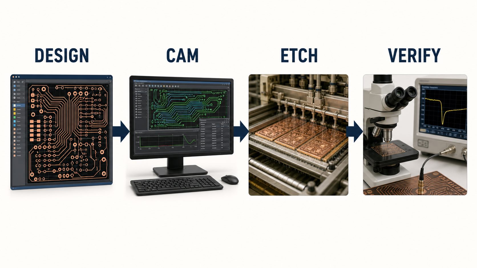
- Step 1: Confirm the stackup and copper definition. Separate starting foil, plated copper, and required finished copper.
- Step 2: Measure the true minimum features. Review isolated neck-down areas, BGA escape zones, plane clearances, and dense routing by layer.
- Step 3: Apply layer-specific working compensation. Use validated factory rules rather than a universal web value.
- Step 4: Recheck clearances after compensation. Widening working traces must not close spaces below the process limit.
- Step 5: Control etching and inspect output. Monitor the process and verify finished geometry using suitable measurement or microsection sampling.
- Step 6: Validate controlled impedance where required. Use the approved stackup and test plan, not only nominal CAD dimensions.
This review belongs inside a broader PCB DFM process, because trace compensation can interact with spacing, pads, hole registration, solder mask, and assembly features.
Which Etching Defects Point to Poor Process Control?
Etching defects become actionable when the observed geometry is connected to a likely cause and a verification step. A single narrow point does not prove one root cause, but the defect pattern can direct the investigation.
| Observed issue | Possible cause | Production impact | Check |
| Trace top is consistently too narrow | Excess lateral attack or insufficient working compensation | Resistance and impedance shift | Measure width by layer and review etch profile |
| Residual copper between traces | Incomplete clearing or local process imbalance | Reduced isolation or shorts | AOI/electrical test and section the affected area |
| Irregular neck-down | Imaging defect, resist damage, debris, or local etch variation | Open-circuit or current-density risk | Compare artwork, AOI image, and finished copper |
| Panel-edge and panel-center differ | Nonuniform spray, chemistry, loading, or transport conditions | Lot variation and poor capability | Use mapped measurements across the panel |
| Impedance coupon misses target | Trace geometry, dielectric, copper, or model mismatch | Signal-integrity failure | Correlate TDR result with microsection and stackup |
What Should You Put in the Fabrication Drawing and RFQ?
A useful fabrication package states the required finished result and gives the factory enough context to select and verify its process. Use this checklist before requesting a quote or releasing the build:
- Gerber or ODB++ copper data with matching revision identification.
- NC drill files and a fabrication drawing.
- Layer stackup, material requirement, and board thickness.
- Starting and/or finished copper requirements stated without ambiguity.
- Minimum trace and space by relevant layer, including localized neck-down areas.
- Controlled-impedance targets, tolerances, layers, reference planes, and net list.
- Finished trace-width tolerance where it is functionally critical.
- Request for coupon, TDR report, microsection, or dimensional evidence when required by the project.
- Instruction that CAM changes beyond agreed compensation require engineering approval.
Send these details before price approval. A quote based only on a zip file and board quantity may not expose whether fine features, heavy copper, or tight impedance need a different production route.
How Should You Review a Fine-Line or Impedance PCB Before Release?
Release review should connect the electrical target, physical geometry, and fabricator capability in one loop. The board is ready only when the minimum features remain manufacturable after realistic compensation and the verification plan can prove the finished result.
- Step 1: Locate every minimum trace, space, and fine-pitch breakout.
- Step 2: Confirm copper requirements and distinguish inner from outer layers.
- Step 3: Review impedance nets with the intended stackup and reference planes.
- Step 4: Ask the selected fabricator to confirm compensated capability and any clearance conflict.
- Step 5: Resolve engineering questions before freezing purchase data.
- Step 6: Define the inspection, coupon, microsection, electrical test, or TDR evidence needed for acceptance.
A calculator can estimate sensitivity, but the release decision must use the actual supplier’s materials, equipment, compensation rules, and inspection method.
FAQs About PCB Etch Factor
Is a higher PCB etch factor always better?
A higher etch factor generally means less lateral undercut relative to copper depth, but it is not a complete board-quality score. Finished trace width, spacing, sidewall condition, uniformity, adhesion, electrical test, and impedance verification still matter. Compare the finished requirement and evidence rather than approving a board from one ratio.
Is etch factor the same as etch compensation?
No. Etch factor describes the relationship between vertical etching and lateral undercut. Etch compensation is the production-data adjustment used to offset expected process loss so the finished copper meets the intended dimensions.
Does the same compensation apply to every PCB layer?
Not necessarily. Inner and outer layers can have different copper constructions and process routes. Copper weight, plating, feature density, and layer artwork can also change the required working allowance. Compensation should be based on the factory’s layer-specific process.
Can I calculate the exact finished width from a generic etch factor?
You can make a first-order sensitivity estimate, but not an exact production prediction. Real cross-sections, plating, bath condition, resist, panel location, and factory compensation affect the result. Use the estimate to identify risk and then request DFM confirmation.
Why does heavy copper need wider traces and spaces?
More copper generally takes longer to clear during subtractive etching, increasing the absolute opportunity for lateral attack. The factory may need more working allowance, which also consumes space. Confirm minimum features for the actual finished copper rather than applying a standard thin-copper table.
How is etch factor checked in production?
Factories may use optical dimensional measurement, AOI data, process coupons, microsections, or other controlled measurements. The appropriate evidence depends on the board and acceptance plan. For impedance boards, a TDR result may be correlated with the stackup and cross-section.
Does solder mask change the etch factor?
Solder mask is normally applied after the copper pattern is formed, so it is not the resist that defines the subtractive copper etch. Imaging resist and copper-processing conditions control that step. Solder mask can still affect the final impedance model for some outer-layer structures.
What should I ask a PCB supplier before approving fine lines?
Ask for minimum finished trace/space at the specified copper weight, whether the limit differs by layer, how controlled impedance is adjusted and verified, what CAM changes require approval, and what inspection or coupon evidence can be supplied.
Send Finished-Dimension and Stackup Requirements for DFM Review
PCBTRY is a suitable manufacturing review option when a design combines fine traces, heavy copper, controlled impedance, HDI escape routing, or tight finished-width requirements. Send Gerber or ODB++ data, drill files, stackup, copper requirements, impedance table, critical tolerance notes, quantity, and inspection requirements to [email protected]. The engineering review can check whether the released geometry leaves enough margin for CAM compensation and the intended production process before quotation and fabrication.



3 Comments
Semi-Additive Process vs Subtractive Etching: PCB Fabrication DFM Differences - thindry pcb manufacturer · 08/24/2026 at 02:42
[…] feature width, etch chemistry and compensation is a practical DFM issue; see PCBtry’s guide to etch factor, undercut and CAM compensation for the related conventional-etch […]
HDI PCB Manufacturing Process: Microvias, Lamination and Testing - thindry pcb manufacturer · 08/24/2026 at 16:10
[…] 2. Core and inner-layer fabrication. The inner core is imaged, etched and inspected before it becomes buried inside the build. Finished conductor width matters more than the artwork alone because etch compensation must account for copper thickness and process behavior. Inner-layer AOI catches opens, shorts and pattern defects before lamination makes repair impractical. See how etch compensation protects finished trace width. […]
Outer Layer PCB Process: Imaging, Copper Plating and Etch Checks - thindry pcb manufacturer · 09/08/2026 at 18:29
[…] The etcher dissolves exposed base copper while tin protects the required pattern. Spray balance, chemistry condition, conveyor behavior, copper loading, and panel orientation influence lateral attack and removal rate. Because etching removes copper sideways as well as downward, the imaged width is not automatically the finished width. Fine lines beside large copper areas are especially sensitive to local loading and the PCB etch factor. […]