




How should a beginner learn PCB design?
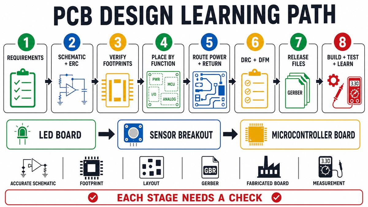
Learn PCB design by completing small boards through the full cycle: understand the circuit, draw a checked schematic, verify footprints, place and route with real manufacturing rules, run ERC/DRC, review outputs, order a small build and test the result. Software commands are only one layer of the skill; the goal is a board that can be fabricated, assembled and debugged.

Start with enough circuit knowledge to predict behavior
Before layout, learn voltage, current, resistance, power, polarity, series/parallel paths, pull-ups, decoupling and basic transistor/IC use. You should be able to explain what each component does and estimate expected voltages. Copying a schematic you cannot explain makes debugging guesswork.
Choose one complete PCB tool and stay with it
KiCad, EasyEDA, Altium and other tools can implement the core workflow. Choose based on access, documentation, collaboration and manufacturer-neutral export needs. Avoid changing tools during the first projects; learn symbols, footprints, net classes, ERC/DRC and fabrication outputs in one environment.
Follow the complete design workflow
| Stage | Skill to learn | Pass condition |
|---|---|---|
| Requirements | Voltage, current, connectors, size, environment | Written constraints |
| Schematic | Logical nodes and component values | Explained circuit plus ERC review |
| Footprints | Package, pin map and courtyard | Datasheet/physical verification |
| Placement | Functional grouping and mechanics | Connectors, decoupling and clearance reviewed |
| Routing | Power, return paths and signals | Rules met; critical paths reviewed |
| Release | Gerber/drill/drawing/BOM | Independent output inspection |
| Build | Assembly and first power | Controlled bring-up checklist |
| Feedback | Compare prediction to measurement | Revision notes captured |
Project 1: design a protected LED board
Use a connector, reverse-polarity protection where appropriate, resistor and LED. Calculate current, verify LED/diode orientation and create test points. This teaches the full source-to-return loop, polarity markings, through-hole or simple SMD footprints and a current-limited first-power check.
Project 2: build a regulated sensor breakout
Add an input connector, regulator, decoupling capacitors, sensor IC and output header. Learn pin mapping, local bypass placement, ground references, thermal considerations and interface pull-ups. Write expected input/output voltages before fabrication.
Project 3: make a small microcontroller board
Add programming/debug access, reset, clock where needed, decoupling, regulator and one interface. Learn component placement by function, return-path continuity, connector protection and firmware bring-up. Avoid high-speed, mains or high-power designs as a first complex project.
Verify every symbol, footprint and pin map
Open the manufacturer datasheet and check pin numbers, package code, pitch, body dimensions, pad recommendations, polarity and exposed pad. Print a 1:1 footprint or compare it with a physical part when possible. Library availability is not proof that the footprint matches your MPN.
Place components by function and mechanics
Fix board outline, holes and connectors first. Group power entry/protection/regulation, keep decoupling close to IC power pins, preserve access to test/program points and consider enclosure height. Placement determines whether routing and assembly will be straightforward.
Route power and return paths before easy signals
Set trace widths and clearances from current, voltage and fabricator capability. Keep signal return paths continuous, avoid unnecessary plane splits and add ground transitions when signals change reference layers. Route critical nets intentionally, then ordinary signals.
Use ERC and DRC as questions, not magic approval
Configure rules, run the checks and resolve every item as a real error or documented exception. ERC/DRC cannot detect a wrong component value, swapped connector definition, unsuitable stackup or poor return path when the database itself says those choices are valid.
Design with manufacturer capabilities in mind
Obtain limits for trace/space, hole sizes, annular rings, board thickness, copper, mask dams and special processes before routing. Use comfortable standard rules for early projects. A DFM review complements DRC by checking the released design against a fabrication process.
Inspect fabrication and assembly outputs independently
- Gerber or ODB++ layers and outline
- NC drill files and plated/non-plated intent
- Stackup and fabrication drawing
- BOM with exact manufacturer part numbers
- Centroid/placement data and assembly drawings
- Polarity and pin-1 markings
- Test points, programming method and acceptance plan
Use a viewer independent of the layout editor so missing, mirrored or extra layers are visible before ordering.
Plan first-board bring-up before ordering
- Inspect the unpowered assembly.
- Check resistance between major rails and ground.
- Use a current-limited source.
- Verify power rails before installing optional loads or enabling subsystems.
- Program firmware through documented access.
- Test one functional block at a time.
- Record expected and measured values.
Use a review checklist before release
| Review | Question |
|---|---|
| Electrical | Can every circuit block and expected voltage be explained? |
| Library | Were symbols, footprints and pin maps checked against datasheets? |
| Mechanical | Do outline, holes, connectors and heights fit the enclosure? |
| Layout | Are power, return paths, decoupling and critical signals intentional? |
| Manufacturing | Do rules and files match supplier capability? |
| Assembly | Are BOM, polarity and placement data unambiguous? |
| Test | Is safe bring-up and pass/fail criteria defined? |
PCB design learning FAQ
Do I need to study electronics before PCB design?
Learn enough to understand and predict the circuits you lay out. PCB software cannot validate the intended electrical behavior for you.
Which PCB software is best for beginners?
The best first tool is one you can access, document and use through schematic, layout, checks and standard manufacturing outputs. Staying with one workflow matters more than chasing tools.
Should my first PCB use SMD components?
Simple larger-pitch SMD parts are reasonable when you can assemble them. Choose packages that match your tools and inspection ability.
How long does it take to learn PCB design?
There is no fixed time. Measure progress by completed design-build-test cycles and fewer undocumented assumptions, not video hours.
Can I copy an open-source PCB?
Respect its license and verify every design choice. Reproducing files without understanding them teaches little and can preserve old errors.
What is the difference between ERC, DRC and DFM?
ERC checks schematic logic rules, DRC checks layout geometry/rules, and DFM reviews released data against a manufacturing process.
When should I move beyond two layers?
Move when routing density, references, EMC, power integrity or mechanics justify it. Layer count should solve a defined problem.
What makes a good beginner project?
It has low voltage, few parts, measurable expected behavior, accessible test points and affordable replacement components.
What should I send for a DFM review?
Send fabrication data, drill files, stackup, drawing and constraints; add BOM, centroid and assembly drawing for PCBA review.
Get feedback before ordering the first board
Independent review catches assumptions that software accepts. Send your fabrication package, stackup, drawings and questions through the PCBTRY contact page for DFM and quotation feedback before committing the first build.



0 Comments