




A single layer PCB manufacturing process converts one-sided copper-clad laminate into a tested circuit board by imaging the circuit pattern, removing unwanted copper, drilling or punching holes, applying solder mask and legend, finishing exposed pads, profiling, and inspecting the result. It avoids multilayer lamination and interlayer-via construction, but that simplicity makes conductor geometry, hole-to-pad registration, laminate choice, and etch control especially important.
PCBTRY can review Gerber data, drill files, fabrication drawings, material requirements, copper weight, surface finish, outline tolerances, and test requirements before production. For a manufacturability review and quotation, send the current file set through the PCBTRY contact page.
What Is a Single Layer PCB?
A single layer PCB has conductive circuitry on one side of an insulating base material. Components may be mounted on the opposite side for through-hole assembly or on the copper side for surface-mount assembly, depending on the product design. The board may use FR-4, paper-based laminate, aluminum-backed material, or another qualified substrate, but “single layer” describes the copper-layer count rather than the base material.
Because there is no second routing layer, traces cannot cross without a jumper, zero-ohm link, or design change. A simple layer count can therefore create difficult routing, narrow neck-downs, congested pads, or long return paths if the circuit was not designed for one-sided fabrication.
When Does a Single Layer PCB Make Sense?
A single-layer construction makes sense when circuit density is low, routing can remain on one copper side, electrical performance does not require dedicated plane layers, and the material/process choice fits the mechanical and thermal load. It is common in simple controls, power supplies, LED products, appliances, toys, and high-volume consumer assemblies where the layout is intentionally optimized for the structure.
Do not choose one layer only because it sounds cheaper. If the design needs many jumpers, very narrow conductors, crowded pads, or poor return-current paths, a two-layer board may reduce assembly work and risk. Compare the complete assembled cost and yield, not only the bare-board price.
How Does the Single Layer PCB Manufacturing Process Work?
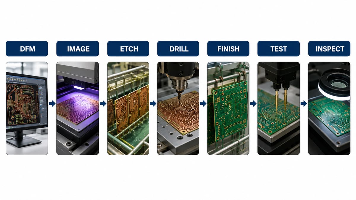
The process keeps all circuit imaging and etching on one copper face, while the exact order of drilling, mask, legend, finish, and profiling depends on the factory route and material. A controlled production flow usually includes the following connected operations.
1. Engineering review and CAM preparation. The manufacturer compares the copper image, solder-mask openings, legend, drill data, board outline, dimensions, material, copper weight, finish, and special notes. CAM engineers panelize the design and create imaging, drilling, routing, inspection, and electrical-test data. Conflicting revisions or an outline that does not match the route data can create scrap before physical processing begins, so buyers should approve clarified assumptions rather than let the factory guess.
2. Laminate selection and panel preparation. The factory selects the approved copper-clad material and cuts it into process panels. Base thickness, copper foil, flammability requirement, mechanical strength, thermal demand, punching route, and assembly temperature all affect the choice. Surface contamination or damaged copper can prevent photoresist adhesion and later appear as broken or rough conductors.
3. Surface cleaning and photoresist application. The copper surface is cleaned and conditioned before dry-film or liquid resist is applied. The resist must contact the copper uniformly without trapped particles, wrinkles, or weak adhesion. Poor preparation can let etchant attack protected copper or leave unwanted copper after development.
4. Imaging, exposure, and development. Direct imaging or artwork exposure transfers the circuit pattern into the resist, then development removes the intended areas. Registration, exposure energy, artwork compensation, and resist condition determine whether pads and traces match the production data. Underexposure can weaken features; overexposure or poor focus can distort fine gaps.
5. Copper etching and resist stripping. Etchant removes unprotected copper, leaving the intended one-sided circuit. Chemistry condition, spray uniformity, conveyor speed, copper thickness, and pattern density influence the result. Excess lateral attack narrows conductors and creates undercut; incomplete etching leaves copper that can bridge adjacent nets. The resist is stripped only after the copper image is complete.
6. Optical inspection of the etched image. The circuit image is checked for opens, shorts, nicks, protrusions, pinholes, residual copper, and dimensional loss. AOI may be used when the design, volume, or process plan justifies it; visual or other inspection routes may be used for simpler work. The buyer should define acceptance through the drawing and applicable workmanship requirement, not assume that one inspection method fits every product.
7. Drilling, punching, or mechanical hole creation. Component leads, mounting points, tooling features, and slots are drilled or punched according to the approved data. Tool wear, panel movement, burr formation, and material behavior influence hole quality and registration. Most holes in a basic single-sided board are non-plated; if conductive hole walls are required, the construction and process route must be stated explicitly rather than implied by a drill file.
8. Solder mask and legend. Solder mask protects most copper and controls exposed soldering areas. The mask image must align with pads without covering solderable land or exposing excessive conductor. Legend adds reference designators, polarity, and assembly markings, but it must not print over pads or other prohibited areas.
9. Surface finish. The finish protects exposed copper and provides a solderable interface. HASL, lead-free HASL, OSP, ENIG, immersion tin, or another approved option may be used depending on component pitch, storage, assembly process, cost, and customer requirements. Finish selection should be documented because flatness, shelf handling, rework, wire bonding, or contact use can change the decision.
10. Profiling, electrical test, final inspection, and packing. Routing, scoring, punching, or another approved method creates the final outline and panel format. Electrical testing checks the supplied netlist or derived circuit for opens and shorts. Final inspection verifies dimensions, hole condition, markings, finish, cleanliness, solder-mask registration, and packaging requirements before release.
Which Materials Are Used for Single Layer PCBs?
Material choice should follow the electrical, mechanical, thermal, flammability, assembly, and volume requirements. A low-cost paper-based laminate may fit a mature appliance design, while FR-4 may be preferred when stiffness, moisture resistance, or assembly conditions demand it. Aluminum-backed single-layer boards address a different thermal path and require an insulated dielectric between copper and metal.
| Material family | Why it may be selected | What the buyer should confirm |
| FR-4 | General mechanical and electrical performance | Grade, thickness, copper, flammability and assembly temperature |
| Paper phenolic / composite laminate | Cost-sensitive, established high-volume products | Punchability, moisture behavior, heat exposure and required rating |
| Aluminum-backed substrate | Heat spreading for LED or power applications | Dielectric system, thermal path, isolation and mechanical processing |
| Specialty laminate | Application-specific electrical, thermal or mechanical need | Availability, validated process route and supplier evidence |
How Do Imaging and Etching Control Trace Quality?
Imaging defines where copper should remain, while etching determines how accurately that pattern survives on the finished panel. The two steps must be controlled together. A perfect digital image cannot compensate for poor resist adhesion or excessive lateral etching, and stable chemistry cannot correct a misregistered exposure.
Engineers should focus on the finished conductor and spacing requirements rather than only the nominal CAD values. Copper thickness, conductor density, panel position, resist profile, and etch compensation affect the result. When conductors neck between pads, ask whether the released geometry stays inside the supplier’s confirmed capability after compensation.
Are the Holes Plated on a Single Layer PCB?
Basic single-layer boards normally use non-plated holes because there is no opposite copper layer to connect. Those holes still need controlled diameter, position, burr, breakout, and mechanical quality. Component leads are soldered to pads on the copper side, and the joint must wet the lead and land correctly.
If a design requires plated holes for mechanical retention, component soldering, or another reason, state that requirement in the drawing and quotation package. Do not use the word “via” casually: a normal via is intended to connect conductive layers, which is not the usual function in a true one-layer board.
How Should Surface Finish Be Selected?
Select the surface finish from the assembly method, pad geometry, storage plan, regulatory requirement, contact function, and cost target. HASL can be practical for many through-hole or less demanding pad geometries; flatter finishes may be considered for fine-pitch SMT. OSP offers a thin, flat coating but handling and assembly planning matter.
Put the finish name and any relevant requirement in the fabrication drawing. “Standard finish” is ambiguous and can lead to a quotation that cannot be compared fairly with another supplier’s offer.
What Tests Verify Single Layer PCB Quality?
Quality verification combines image inspection, dimensional checks, hole and profile inspection, surface-finish review, and an electrical open/short test. The test plan should reflect the product risk and customer specification. A visually clean board can still contain an electrical open, while a board that passes continuity can still have a dimensional or solderability problem.
| Potential problem | Useful evidence | Buyer decision |
| Narrowed or broken trace | AOI/visual result plus electrical test | Confirm finished geometry and acceptability |
| Residual copper bridge | Optical inspection and short test | Reject unapproved conductive connection |
| Hole-to-pad breakout | Dimensional and registration inspection | Compare with drawing and applicable criteria |
| Mask on solderable pad | Mask registration inspection | Assess assembly risk and disposition |
| Poor or damaged finish | Finish inspection and specified acceptance evidence | Confirm solderability and storage suitability |
What Manufacturing Failures Are Most Common?
The most consequential failures are opens from over-etch or resist damage, shorts from incomplete etching, hole misregistration, pad breakout, burrs, solder-mask misalignment, outline error, poor finish coverage, and contamination. These defects often trace back to inconsistent input data, unstable surface preparation, process drift, worn mechanical tools, or inadequate inspection.
A buyer should ask for evidence tied to the risk rather than a generic statement that the board passed QC. That may include electrical-test confirmation, first-article dimensions, an inspection report, material identification, finish confirmation, or retained coupon/sample evidence when the purchase specification requires it.
How Does PCB Design Affect Yield and Reliability?
A design with reasonable trace width and spacing, adequate annular land, copper-to-edge clearance, clear polarity marks, accessible test points, and a manufacturable panel arrangement gives the process more margin. A one-layer board with forced routing and many narrow necks may be inexpensive on paper but sensitive to etch variation and assembly damage.
Review jumper count, current paths, heat concentration, mechanical loads, creepage/clearance requirements, and component lead access before release. Where the electrical or mechanical compromises become excessive, upgrading to two layers is an engineering decision—not a manufacturing failure.
What Affects Cost and Lead Time?
Cost and lead time depend on material, panel utilization, copper weight, hole count and method, outline process, solder mask, legend, finish, testing, tooling, quantity, inspection documentation, and revision stability. A special material or punching tool may dominate a high-volume program, while engineering clarification and setup matter more for a small prototype order.
Ask suppliers to quote the same revision, panel condition, finish, test scope, packaging, and documentation. Otherwise, two prices may describe different deliverables.
What Files Are Needed for an RFQ?
A usable RFQ identifies both the circuit data and the manufacturing assumptions. Send:
- Copper, solder-mask, and legend Gerber files.
- NC drill and slot data with plated/non-plated intent stated clearly.
- Board outline and dimensioned fabrication drawing.
- Material, thickness, copper weight, solder mask, legend, and finish requirements.
- Panelization, scoring, routing, punching, tooling-hole, or breakaway requirements.
- Applicable workmanship, test, inspection, packaging, and traceability requirements.
- Quantity, revision, target schedule, and assembly constraints that affect the board.
How Do You Choose a Single Layer PCB Manufacturer?
Choose a manufacturer that can explain the exact route for your material and volume, review one-sided routing risks, control imaging and etching, distinguish plated from non-plated hole requirements, and provide test evidence that matches the purchase specification. A low quote without assumptions, test scope, or material clarity is difficult to evaluate.
Ask how the supplier manages CAM questions, first-article dimensions, material substitution, etch control, punching or routing tools, electrical test, nonconforming product, and revision control. PCBTRY’s PCB manufacturing service can be used as an engineering-review and comparison-quote path when the confirmed capabilities fit the project.
Frequently Asked Questions
Is a single layer PCB the same as a single-sided PCB?
In normal purchasing use, both terms describe a board with one conductive copper layer. Confirm the drawing because component placement and soldering arrangements may still differ.
Does a single layer PCB require lamination?
It starts from an already manufactured copper-clad laminate, but it does not require the multilayer lay-up and bonding cycle used to combine several circuit layers. Specialty constructions may have other bonding operations, which should be specified separately.
Can surface-mount components be used?
Yes. SMT components can be placed on the copper side when the layout, assembly process, thermal profile, and inspection access support it.
Are electrical tests necessary for simple boards?
An open/short test is valuable because visual appearance alone cannot prove net continuity and isolation. The required sampling or test scope should follow the purchase specification and product risk.
Why do single-layer traces become too narrow after etching?
Lateral etch, resist profile, copper thickness, chemistry, and process time can reduce finished conductor width. The supplier should evaluate the released geometry against confirmed finished-feature capability.
Can single layer PCBs use ENIG?
They can use ENIG or other finishes when the base material, design, assembly process, and specification support it. Select the finish for actual pad and product needs rather than layer count alone.
When should I change to a two-layer board?
Consider two layers when one-sided routing creates excessive jumpers, poor return paths, cramped conductors, assembly complexity, or unacceptable electrical and mechanical compromises.
What should I send for a quotation?
Send Gerber files, drill/slot data, outline, fabrication drawing, material and finish requirements, quantity, test scope, panel needs, and revision information. Identify non-plated holes explicitly.
Request a Manufacturing Review
Send the Gerber package, drill data, drawing, material, copper, finish, test requirements, quantity, and assembly constraints through the PCBTRY contact page. Ask the engineering team to flag one-layer routing compromises, hole intent, finished conductor risk, panel/tooling assumptions, and any item that must be clarified before quotation.



0 Comments