




Multilayer PCBs place patterned copper layers inside a laminated dielectric stack so designers can route dense circuits, create reference planes, and control electrical behavior in less area. They are used in industrial controls, communications, computing, medical electronics, automotive modules, and other products where a two-layer board cannot provide enough routing or power integrity. Their manufacturing risk is cumulative: an inner-layer defect, registration shift, resin-fill problem, or weak plated hole may remain hidden after lamination.
A useful fabrication review starts with the complete stack-up, material system, copper weights, finished thickness, via structure, impedance requirements, tolerances, and acceptance evidence. Send Gerbers, NC drill and outline files, stack-up, drawings, quantities, and test requirements through PCBTRY’s engineering contact for DFM review and quotation.
What Is the Multilayer PCB Manufacturing Process?
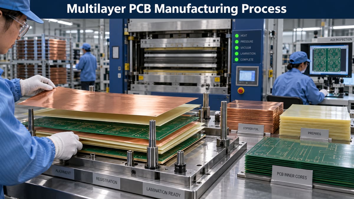
The multilayer PCB manufacturing process images and inspects inner-layer cores, bonds them with prepreg and copper foil, drills the laminated panel, metallizes the holes, forms the outer circuitry, and finishes and tests the board. Unlike a two-layer board, internal copper cannot be directly repaired or inspected after lamination, so in-process verification and coupon evidence matter.
How Does the Multilayer PCB Manufacturing Process Work?
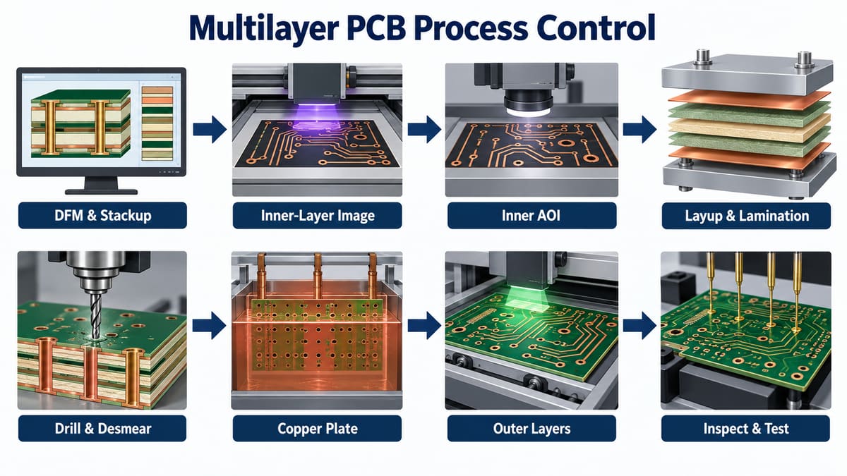
1. Engineering review and stack-up release. CAM engineers reconcile layer order, polarity, drill spans, copper weights, dielectric targets, impedance notes, finished thickness, profile, and fabrication tolerances. A swapped plane layer or ambiguous blind-via span can make a correctly processed panel electrically wrong, so the controlled stack-up and build notes must be approved before tooling.
2. Inner-layer imaging and etching. Each copper-clad core receives the inner-layer image, is developed, etched, and stripped. Imaging compensation accounts for expected dimensional movement. Over-etching narrows conductors; under-etching can leave shorts. Registration targets and test coupons travel with the production pattern.
3. Inner-layer AOI and treatment. AOI checks opens, shorts, nicks, spacing, and pattern registration while copper is still visible. Accepted cores then receive the specified surface treatment to support bonding. AOI cannot prove future resin fill, layer-to-layer registration, or plated-hole integrity, so it is one gate rather than final proof.
4. Layup and lamination. Operators arrange cores, prepreg, and outer copper foil in the released order and align them with the selected registration method. The press cycle applies controlled heat, pressure, and vacuum. Incorrect layup, contamination, insufficient resin flow, trapped gas, or uneven cure can cause delamination, voids, thickness variation, and poor dielectric spacing.
5. Registration verification, drilling, and desmear. After lamination, targets or imaging systems locate the internal pattern so holes land correctly. Drilling creates plated and non-plated features; tool wear and debris affect wall quality. Desmear removes resin from exposed copper interfaces. Excessive removal can damage dielectric; insufficient cleaning can weaken interconnection.
6. Hole metallization and copper plating. A conductive seed layer is established on nonconductive hole walls, then copper is built to the required structure. Voids, folds, weak adhesion, or insufficient deposit can create latent opens during assembly or service. Coupons and microsections provide evidence that cannot be obtained from surface inspection alone.
7. Outer-layer imaging, pattern plating, and etching. The external circuitry is imaged and plated, protective metal is applied where the process requires it, and unwanted copper is etched away. Registration now must align outer pads, drilled holes, and internal targets. AOI and dimensional checks identify conductor and annular-ring risks before solder mask.
8. Solder mask, finish, legend, and profiling. Solder mask openings are aligned to pads, exposed copper receives the specified surface finish, identification is applied, and the board is routed or scored. Finish choice must match assembly and contact needs. Mask shift, contaminated pads, damaged edges, and wrong profile dimensions directly affect assembly yield.
9. Electrical inspection and final acceptance. Electrical test verifies continuity and isolation against the netlist. Final inspection may include dimensions, bow/twist, impedance coupons, microsections, cleanliness, finish checks, and customer-specific reports. Electrical test proves the tested net condition; it does not replace structural evidence for hidden interfaces.
How Is a Multilayer PCB Stack-Up Designed?
The stack-up balances electrical targets, copper distribution, dielectric thickness, manufacturability, and mechanical symmetry. Reference planes should support the intended return paths, while copper and dielectric construction should avoid unnecessary imbalance that can contribute to bow, twist, or lamination stress.
| Stack-up input | Manufacturing question | Evidence to approve |
|---|---|---|
| Layer count/order | Are signal and plane polarities unambiguous? | Numbered controlled stack drawing |
| Core and prepreg | Can the material system fill copper patterns and meet thickness? | Material family and construction |
| Copper distribution | Is the build reasonably balanced? | Copper review and panel strategy |
| Impedance | Which traces, references and coupons are controlled? | Trace table and coupon plan |
| Via structure | Which holes are through, blind, buried, filled, or stacked? | Drill-span table and cross-section |
What Are the Key Manufacturing Challenges?
- Layer registration: cores move during processing and lamination, affecting drill-to-copper alignment.
- Resin distribution: copper density and prepreg selection affect fill, dielectric thickness, and void risk.
- Hole-wall integrity: drilling, desmear, metallization, and plating act as one reliability chain.
- Material compatibility: mixed constructions must tolerate lamination and assembly thermal history.
- Hidden defects: internal interfaces require in-process AOI, coupons, X-ray or microsection evidence as specified.
How Does Design Affect Reliability?
Annular-ring allowance, via aspect ratio, pad geometry, copper balance, plane clearances, impedance reference continuity, and thermal reliefs all influence yield and lifetime. More layers do not automatically improve performance: a poorly planned return path or unnecessary sequential lamination can increase risk without adding useful function.
Ask the fabricator to return the proposed stack-up and identify any material substitution, impedance adjustment, drill change, or tolerance conflict before production. Record approved changes in the fabrication drawing rather than leaving them in email.
What Tests Ensure Multilayer PCB Quality?
| Check | What it finds | Limit |
|---|---|---|
| Inner/outer AOI | Visible conductor defects and registration issues | Cannot prove hidden bond or plated-hole structure |
| Electrical test | Opens and shorts against the netlist | Does not measure every structural weakness |
| Microsection/coupon | Plating, interfaces, registration and dielectric structure | Represents defined coupon/sample locations |
| Impedance coupon | Controlled-line result for agreed structures | Requires correct coupon-to-product correlation |
| Dimensional inspection | Profile, holes, thickness and critical geometry | Only useful when critical tolerances are identified |
How Long Does Multilayer PCB Manufacturing Take?
Lead time depends on material availability, layer count, sequential lamination cycles, blind/buried vias, controlled impedance, hole filling, special finishes, coupons, testing, and approval delays. Ask for a schedule that separates engineering questions, material procurement, fabrication, special testing, and shipment; do not compare suppliers using an undefined “standard lead time.”
How Do You Choose a Multilayer PCB Manufacturer?
Evaluate the supplier against your actual construction. Ask how stack-ups are controlled, inner layers are inspected, registration is measured, press recipes are released, drill/plating quality is verified, and coupon results are linked to the lot. The quote should identify assumptions, exceptions, test scope, and material substitutions.
- Will engineering return a controlled stack-up and drill-span table?
- Which inner-layer checks occur before lamination?
- What coupon or microsection evidence is included?
- How are impedance adjustments approved?
- How are nonconforming panels contained and traced?
Frequently Asked Questions
What files are needed for a multilayer PCB quote?
Provide Gerbers, drill and route files, stack-up, fabrication drawing, netlist, quantities, copper weights, finish, impedance table, tolerances, and test/report requirements.
Why inspect inner layers before lamination?
Once bonded, internal conductor defects are difficult to access. AOI removes defective cores before they become expensive completed panels.
What causes multilayer PCB delamination?
Contributors include contamination, moisture, material mismatch, incomplete cure, poor surface preparation, voids, and thermal stress. Failure analysis must identify the interface and process history.
Does electrical test prove via reliability?
It confirms connectivity at the time and condition of test. Structural coupons, microsections, thermal conditioning, or reliability tests may be needed for the intended risk.
What is layer registration?
It is the alignment of internal and external copper patterns to each other and to drilled features. Poor registration reduces available annular ring and can threaten isolation.
Are more PCB layers always better?
No. Add layers only when routing, planes, impedance, EMC, or power distribution justify the extra construction and process complexity.
Why does copper balance matter?
Uneven copper distribution changes resin demand and mechanical balance. Engineering should review it with the stack-up and panel design.
What should a first-article report include?
Prioritize critical dimensions, stack-up, materials, impedance, hole structure, microsection/coupon results, electrical test, and any customer-defined acceptance evidence.
Send a Manufacturing-Ready Multilayer PCB RFQ
Send the complete fabrication package through PCBTRY’s contact page and request written confirmation of stack-up, materials, via construction, inspection, coupon evidence, and unresolved DFM questions before release.



0 Comments