Blog
How to Read PCB Layout: Layers, Traces and DFM Checks
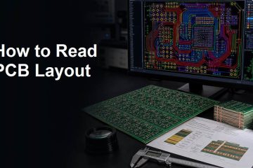
Learn how to read PCB layout files by checking board outline, layers, components, traces, vias, drill files, silkscreen, and DFM issues before fabrication.



Learn how to read PCB layout files by checking board outline, layers, components, traces, vias, drill files, silkscreen, and DFM issues before fabrication.
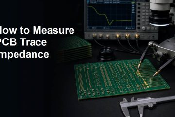
Learn how to measure PCB trace impedance with TDR, test coupons, stackup data, tolerance checks, and controlled impedance DFM review.
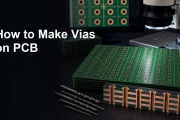
Learn how to make vias on PCB with drilling, copper plating, via types, annular ring checks, aspect ratio limits, and DFM notes before fabrication.

Learn how to make double sided PCB with copper layers, plated vias, alignment, DFM checks, Gerber files and manufacturing review.
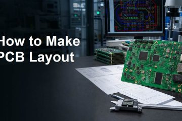
Learn how to make PCB layout from schematic and footprints to placement, routing, DFM checks, Gerber files and manufacturing review.
Learn how to design a PCB board for a circuit, from schematic and footprints to layout, DFM checks, manufacturing files and quote-ready review.
Let’s delve into two core concepts in PCB manufacturing: DFM (Design for Manufacturability) and DFA (Design for Assemblability). They represent the most critical application of the “Concurrent Engineering” and “Design for X” philosophies within the electronics industry. Their goal is to prevent problems at the design source, thereby significantly reducing Read more
If you have any enquiry about quotation or cooperation, please feel free to email us at [email protected] or use the following enquiry form. Oursales representative will contact you within 24 hours. Thank you for your interest in our products.