




What Is a 4 Layer PCB Stackup?
A 4 layer PCB stackup is the order of copper and insulating layers inside a four-layer circuit board. Instead of only top and bottom copper, the board has two outer layers and two internal layers. The internal layers are often used as ground and power planes.
A common practical stackup is Top Signal – Ground Plane – Power Plane – Bottom Signal. This gives better routing space, lower noise and more stable return paths than a simple 2 layer PCB. It is often used for microcontrollers, wireless modules, power circuits, faster digital signals and compact layouts.
The stackup is not just a drawing. It affects impedance, EMI, heat, warpage, drilling, lamination and fabrication cost. A good 4 layer board starts with a stackup that the PCB factory can actually build.
Common 4 Layer PCB Stackup Example
| Layer | Common use | Why it is used |
|---|---|---|
| L1 Top | Signals and components | Short routes from components and controlled signal breakout |
| L2 Inner | Ground plane | Stable return path and shielding below top signals |
| L3 Inner | Power plane or split power | Distributes power and supports decoupling |
| L4 Bottom | Signals and some power routing | Additional routing and secondary component side if needed |
This stackup is popular because it is easy to understand and works well for many general digital boards. The top signal layer references the nearby ground plane. The power plane can support power distribution. The bottom layer gives extra routing space.
It is not always the best choice. RF boards, high-speed differential pairs, dense BGAs, high-current power boards or strict impedance designs may need a more carefully calculated stackup.
Why Ground Plane Placement Matters
The ground plane is the quiet reference layer for many signals. When a signal travels on the top layer, its return current tends to flow on the closest reference plane. If L2 is a continuous ground plane, that return path is short and controlled.
If the ground plane is split or cut by large gaps, return current must detour. That can increase noise, EMI and signal integrity problems. For many 4 layer boards, keeping L2 as a solid ground plane is one of the safest design decisions.
Do not treat the ground plane as leftover copper. It is part of the signal path. A signal trace without a good return path is not a complete design.
When Should L3 Be Power and When Should It Be Ground?
L3 is often used as a power plane, but that is not mandatory. Some designs use two ground planes and route power as traces or pours. This can improve shielding and return paths, especially when power requirements are modest.
| Stackup choice | Good fit | Risk to check |
|---|---|---|
| L2 ground, L3 power | General digital boards with several rails | Power splits should not break important return paths |
| L2 ground, L3 ground | Noise-sensitive or RF-like layouts with modest power | Power routing must still handle current and voltage drop |
| Power near top, ground near bottom | Special routing or component-side needs | May weaken top-layer signal reference if not planned |
The best choice depends on current, noise sensitivity, impedance targets, component placement and routing density. If you are unsure, ask the PCB manufacturer to review the intended stackup before ordering impedance-controlled boards.
4 Layer PCB Stackup and Controlled Impedance
Controlled impedance depends on trace width, copper thickness, dielectric thickness, dielectric constant and the reference plane. On a 4 layer PCB, the distance between L1 and L2 or between L4 and L3 is especially important for microstrip routing.
If you need 50 ohm single-ended traces or 90/100 ohm differential pairs, do not guess the trace width from a generic calculator alone. The factory stackup and material data must match the calculation.
For impedance control, send the target impedance, layer, trace width, spacing, tolerance and stackup requirement. The manufacturer can then confirm whether the proposed structure is manufacturable.
How Copper Thickness Affects a 4 Layer Stackup
Copper thickness affects current capacity, impedance, etching limits and lamination balance. Common finished copper values include 1 oz and heavier copper options, but the right choice depends on current and trace geometry.
Thicker copper can help power handling, but it may require wider spacing and can affect fine trace fabrication. It can also change impedance calculations. Do not increase copper thickness only because it sounds stronger.
If the board has high-current paths, provide current, temperature-rise expectations, trace widths and copper weight requirements. If the board has impedance-controlled signals, confirm the copper thickness with the stackup.
DFM Checks Before You Order a 4 Layer PCB
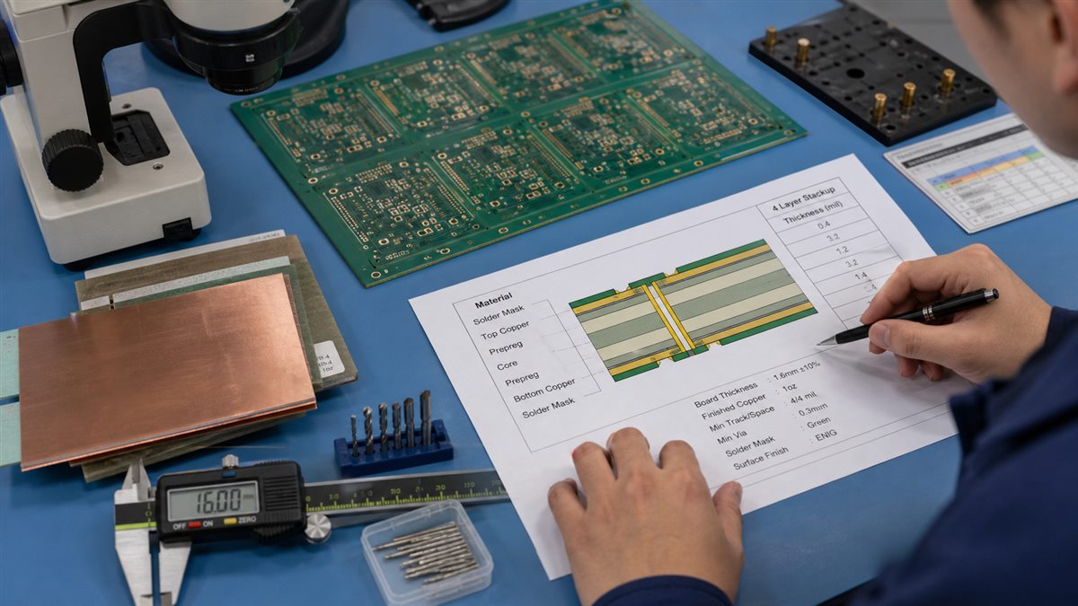
A stackup that looks fine in CAD may still need manufacturing review. The factory checks whether the layer order, dielectric thickness, copper balance, drill structure and finished board thickness are reasonable.
- Confirm total board thickness, such as 1.6 mm or a special thickness.
- Confirm copper weight for each layer.
- Check minimum trace width and spacing.
- Check via drill size, annular ring and aspect ratio.
- Review copper balance to reduce warpage risk.
- Confirm impedance requirements before fabrication.
- Make sure plane splits do not cross critical signal return paths.
Via Planning in a 4 Layer PCB
Vias connect signals between layers. On a standard 4 layer PCB, through vias are common because they are simple and economical. Blind or buried vias are possible in some designs, but they add complexity and cost.
Via size affects routing density and manufacturability. Very small drills can increase cost or reduce yield if they exceed the process comfort zone. Dense via fields near BGAs should be reviewed early.
For most general 4 layer boards, use standard through vias where possible and reserve advanced via structures for designs that truly need them.
Common 4 Layer PCB Stackup Mistakes
| Mistake | Why it matters | Better approach |
|---|---|---|
| Splitting the ground plane under fast signals | Return path detours and EMI risk | Keep a continuous reference plane |
| Choosing trace widths before stackup confirmation | Impedance may be wrong | Confirm material and dielectric thickness first |
| Ignoring copper balance | Warpage and lamination risk | Review layer copper distribution |
| Using advanced vias without need | Higher cost and process complexity | Use standard through vias when possible |
| Assuming every factory uses the same stackup | Material and thickness can differ | Ask for a manufacturable stackup before release |
What to Send the PCB Manufacturer
For a 4 layer PCB quote, send the normal fabrication files and any stackup-specific requirements. If controlled impedance is required, make that clear before fabrication starts.
- Gerber or ODB++ files.
- NC drill files.
- Fabrication drawing.
- Requested layer order and total thickness.
- Copper weight for each layer.
- Material requirement, such as FR-4 grade or Tg requirement.
- Controlled impedance table if needed.
- Surface finish, solder mask color and silkscreen requirements.
FAQ
What is the best 4 layer PCB stackup?
A common and safe general stackup is signal, ground, power, signal. It is not always best for every design, but it works well for many digital boards when L2 is kept as a solid ground plane.
Is a 4 layer PCB better than a 2 layer PCB?
A 4 layer PCB usually gives better routing, ground reference and noise control. It costs more than a 2 layer PCB, but it can reduce layout problems for denser or faster circuits.
Can a 4 layer PCB have controlled impedance?
Yes. Controlled impedance is possible, but the stackup, material, copper thickness, dielectric thickness, trace width and spacing must be confirmed together.
Should the power plane be solid?
It depends on the number of rails and current needs. A power plane can be solid or split, but splits should be planned so they do not disrupt important return paths.
What files are needed for a 4 layer PCB quote?
Send Gerber or ODB++ files, drill files, fabrication drawing, stackup request, copper weight, material requirement and impedance information if applicable.
Ask for Stackup Review Before Fabrication
A 4 layer PCB stackup should be practical for both circuit performance and fabrication. Before releasing files, check the layer order, ground plane, power distribution, copper weight, via structure and impedance needs.
PCBtry can review your PCB fabrication files and confirm whether your requested 4 layer stackup, material, copper weight and impedance targets are suitable for production. Send your Gerber files, drill files, fabrication drawing and stackup notes through the contact page for engineering review.



0 Comments