




What should a China PCB design service actually deliver?
A capable China PCB design service should convert an agreed electrical and mechanical brief into a controlled schematic, verified component library, manufacturable layout, review evidence, and a complete source and production package. The country does not define design quality. Scope, engineering evidence, communication, ownership, and acceptance gates do. Before comparing prices, make every provider quote the same inputs, outputs, revision cycle, and responsibility boundary.

Choose the provider type that fits the project
| Provider type | Often suitable for | Check carefully |
|---|---|---|
| Independent designer | Defined circuit, focused layout task, direct engineer contact | Backup capacity, library process, fabrication support, and handoff completeness |
| Design studio | Schematic, layout, mechanical coordination, firmware or compliance support | Who performs the work, discipline boundaries, and change control |
| Factory-linked design team | Projects intended to move quickly into PCB fabrication or PCBA | Design independence, source-file ownership, component neutrality, and whether rules suit your actual factory options |
| Marketplace contractor | Small, well-bounded tasks with strong buyer oversight | Identity, relevant examples, confidentiality, continuity, and post-release support |
A factory-linked team can shorten DFM feedback, but that advantage is useful only when the design outputs remain controlled and portable. An independent designer may offer broader manufacturing choices, but the buyer must ensure that real fabrication rules are incorporated.
Write a design brief before requesting a quote
A quote based only on “design this board” is not comparable. Prepare a brief that states the product function, interfaces, supply conditions, mechanical envelope, operating environment, expected quantity, regulatory context, test approach, and what work already exists.
- Functional block diagram and required inputs/outputs
- Supply voltage, current, protection, power sequencing, and battery requirements
- Processors, sensors, radios, connectors, displays, motors, or other fixed choices
- Board outline, mounting, connector positions, component height, and enclosure data
- Signal speeds, impedance needs, analog accuracy, noise, EMC, thermal, and isolation concerns
- Target prototype date, production volume, assembly route, and test expectations
- Existing schematic, netlist, CAD data, firmware dependencies, and known problems
- Required deliverables, file formats, review stages, and ownership terms
Separate schematic work from layout work
“PCB design” can mean schematic capture, circuit engineering, component selection, footprint creation, layout, or all of them. State which tasks are included. If the provider receives an approved schematic, define whether it may change the circuit and who approves changes. If circuit design is included, require documented design assumptions, calculations where relevant, datasheet references, and a schematic review before layout begins.
Confirm the component and library process
Every symbol and footprint creates manufacturing risk. Ask how the team verifies pin numbers, package variants, land patterns, polarity, height, lifecycle, and sourcing. Critical or unfamiliar parts should be checked against the manufacturer datasheet and, where possible, a physical sample or qualified library record.
The BOM should use exact manufacturer part numbers and state allowed substitutions. Do not accept a design whose source library depends on an inaccessible personal database without an agreed archive or exported library package.
Set the stackup before critical routing
Layer count alone is not a stackup. The designer needs the intended dielectric arrangement, copper weights, finished thickness, reference-plane strategy, impedance targets, and fabricator capability. For controlled-impedance, high-speed, high-voltage, RF, flex, HDI, or heavy-copper work, involve a suitable fabricator before routing is frozen.
Ask the designer to show which layer references each critical signal and how return paths continue through layer transitions. A later stackup change can alter impedance, spacing, via structure, and EMC behavior.
Agree layout constraints in measurable terms
| Constraint group | Examples to define | Evidence at review |
|---|---|---|
| Fabrication | Trace, clearance, via, annular ring, mask, copper-to-edge | Rule setup and DRC report |
| Electrical | Current paths, impedance, differential pairs, creepage, isolation | Constraint report and routed examples |
| Mechanical | Outline, holes, keepouts, connector direction, height | Dimensioned drawing and 3D fit review |
| Assembly | Courtyard, polarity, fiducials, tooling, rework access | Assembly drawing and placement review |
| Test | Rail, programming, boundary, functional, and fixture access | Test-point map and expected readings |
Use review milestones instead of one final approval
- Brief review: confirm requirements, exclusions, interfaces, risks, files, and acceptance criteria.
- Schematic review: verify circuit function, power, protection, pin mapping, net naming, and test strategy.
- Placement review: check mechanics, functional grouping, thermal paths, sensitive circuits, connectors, and service access.
- Critical-routing review: inspect power, clocks, RF, high-speed, analog, isolation, and return paths before general routing is locked.
- DFM and assembly review: run the target fabrication and assembly rules against the nearly finished design.
- Release review: compare source data, manufacturing outputs, BOM, CPL, drawings, and revision identifiers before approval.
Record comments and dispositions at every milestone. Screenshots in chat are not a substitute for an approved revision.
Make DFM part of design, not a final cleanup
DFM checks whether the design matches a real manufacturing process, but it should begin with the stackup and component choices. Confirm fabrication limits, panel support, surface finish, special vias, controlled depth, impedance, tolerances, solder-mask behavior, assembly clearances, thermal balance, and inspection access. A clean CAD DRC only proves compliance with the rules that were entered.
Protect signal integrity, power integrity, and EMC intent
For relevant projects, ask how the designer controls reference planes, return-current discontinuities, differential-pair geometry, termination placement, decoupling, switching loops, power distribution, layer changes, and connector transitions. The needed analysis depends on edge rate, interconnect length, power demand, noise margin, and product risk. Do not buy simulation as a decorative report; agree what question it must answer and what model assumptions are used.
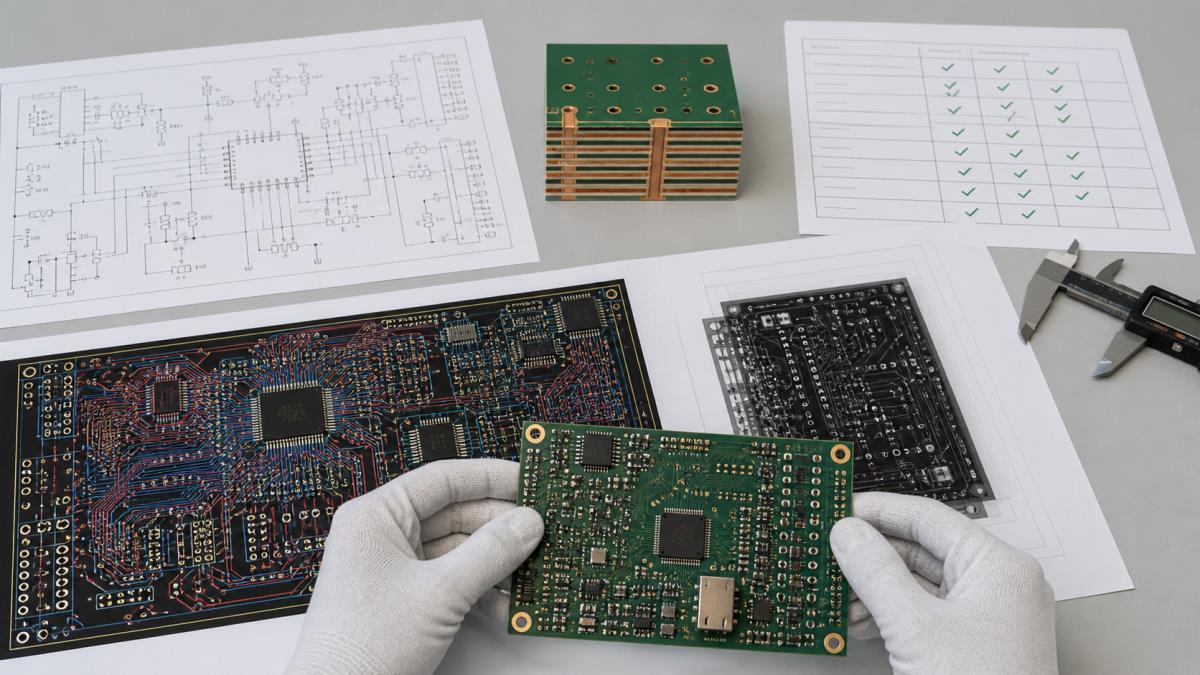
Define source-file ownership and tool versions
The agreement should state who owns editable schematics, PCB layout, libraries, calculations, simulation files, drawings, and generated manufacturing data after payment. Record the CAD tool and version, included libraries, fonts or scripts, and whether third-party licensed content restricts reuse. If the supplier keeps only proprietary source files and gives you Gerbers, future revision and supplier-change options are limited.
Require a complete manufacturing handoff
| Deliverable | Acceptance check |
|---|---|
| Editable schematic and PCB source | Opens in the agreed tool/version with libraries resolved |
| Gerber or ODB++ and drill data | Independent viewer matches copper, mask, legend, outline, and holes |
| Fabrication drawing and stackup | Materials, thickness, copper, finish, tolerances, impedance, and notes agree |
| BOM | Exact MPNs, quantities, references, do-not-fit parts, and substitutions are controlled |
| CPL/centroid and assembly drawings | Coordinates, rotation, side, polarity, and reference designators match the PCB |
| Test and programming information | Test points, expected values, firmware, connector, and procedure are usable |
| Review records | Open issues are resolved, waived with reason, or assigned before release |
Compare quotations on the same scope
Separate engineering fees from fabrication, assembly, components, test fixtures, certification support, and revision work. Note the included number of review cycles, response assumptions, schedule dependencies, and hourly or fixed-price treatment of changes. A lower design fee can create a higher total cost when libraries, DFM, source files, or prototype support are excluded.
Ask for evidence that matches your board
Request anonymized examples or review artifacts from projects with comparable technical risks, not merely attractive PCB renders. For a power board, ask about current and thermal review. For RF or high-speed work, ask how stackup and measurement were handled. For dense PCBA, ask about component library, assembly, inspection, and test coordination. Protect confidential information on both sides.
Watch for these design-service red flags
- A firm price and date before requirements or files are reviewed
- No named reviewer or unclear responsibility for schematic versus layout
- “Any layer count” or “any technology” claims without project-specific questions
- No written stackup, rule source, or fabrication capability confirmation
- Only rendered images are offered as design evidence
- Editable source files and libraries are excluded or ownership is ambiguous
- Gerber generation is treated as proof that the design is correct
- No revision control, review log, DFM record, or release checklist
- Prototype problems are automatically assigned to manufacturing without root-cause review
China PCB design FAQ
How much does PCB design cost in China?
Cost depends on schematic scope, layer count, component count, mechanical constraints, signal and power complexity, required analysis, documentation, and review cycles. Compare written scopes rather than a single board price.
Can a PCB factory also design my board?
Some factories offer design or engineering support. Confirm the exact tasks, engineer qualifications, source-file ownership, design review method, and whether the output remains usable if another factory manufactures it.
What files are needed to start PCB layout?
Typically an approved schematic, BOM or preferred parts, board outline and mechanical constraints, interface definitions, stackup direction, electrical constraints, fabrication rules, and test requirements.
Should I provide the stackup?
Provide performance and mechanical requirements, then agree a manufacturable stackup with the designer and intended fabricator before critical routing.
Who owns the PCB design files?
Ownership follows the written agreement. State explicitly whether editable source files, libraries, drawings, calculations, and manufacturing data transfer to you and when.
Is DRC the same as DFM?
No. DRC checks the design against configured CAD rules. DFM checks compatibility with the intended fabrication and assembly processes, including rules that may not exist in the CAD setup.
How do I review a PCB design if I am not an expert?
Use staged reviews and require direct evidence: requirements mapping, schematic checklist, mechanical fit, stackup, DRC/DFM reports, independent Gerber viewing, and a complete release checklist. Use a separate reviewer for high-risk designs.
Should prototype fabrication be included?
It can improve feedback speed, but keep design acceptance separate from manufacturing acceptance. Define how prototype defects are investigated and who updates controlled source files.
What should I send for a design-service quotation?
Send the functional brief, existing circuit files, mechanical data, interfaces, environment, quantity, compliance context, schedule, required design tasks, expected deliverables, and review requirements.
Request a scoped PCB design and DFM review
Send your functional brief, schematic status, mechanical files, interfaces, expected quantity, target stackup, and required deliverables through the PCBTRY contact page. Ask for a written responsibility matrix and milestone plan covering schematic, layout, DFM, fabrication data, BOM/CPL, testing, editable source files, and prototype support.



0 Comments