




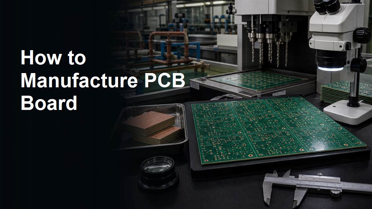
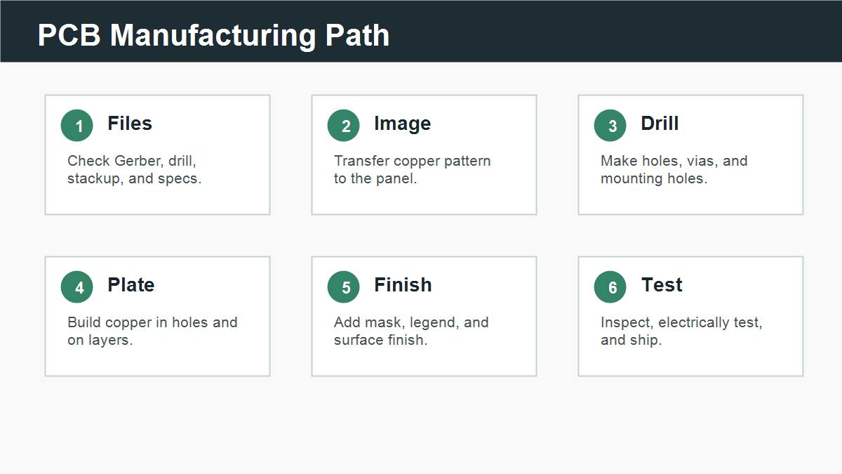
To manufacture a PCB board, the factory first checks the Gerber files, drill files, stackup, material, copper weight, thickness, surface finish, and DFM rules. Then it creates copper patterns, drills holes, plates copper, etches unwanted copper, applies solder mask and silkscreen, finishes exposed pads, routes the board shape, inspects quality, and electrically tests the finished boards.
Think of PCB manufacturing as turning a digital board map into a physical copper-and-laminate product. Each process step exists to answer one practical question: where should copper remain, where should holes connect layers, what needs insulation, and how do we prove the board is buildable.
Start With the Manufacturing Files
The factory cannot manufacture the board from a screenshot. It needs Gerber files for copper, solder mask, and silkscreen, plus drill files for plated and non-plated holes. It also needs board thickness, material, copper weight, surface finish, quantity, and special requirements.
If a file is missing, the factory may ask questions before production. If the wrong file is sent, the board can be manufactured exactly as the file says but still be wrong for the circuit.
Run DFM Before Production Starts
DFM means design for manufacturability. In simple terms, it checks whether the board can be built reliably with the chosen process. The factory checks trace width, spacing, drill size, annular ring, solder mask bridge, copper-to-edge distance, board outline, and special structures.
This step matters because fixing a problem before production is cheaper than scrapping finished panels. For more detail, read PCBTRY’s guide to DFM and DFA in PCB manufacturing.
Create the Copper Pattern
The copper pattern is the real circuit on the board. The factory transfers the design pattern onto copper-clad material, then removes unwanted copper so only the required traces, pads, and planes remain.
For a beginner, imagine starting with a sheet of copper and then keeping only the copper roads that the circuit needs. The Gerber copper layers tell the factory which roads stay and which copper is removed.
Drill Holes and Plate Vias
Drilling creates component holes, mounting holes, and via holes. Plated holes need copper on the hole wall so the top layer, bottom layer, or inner layers can connect electrically. Non-plated holes are mechanical holes without copper connection.
Vias are especially important because they let signals and power move between layers. PCBTRY’s article on how to make vias on PCB explains the drilling and plating logic in more detail.
Add Solder Mask, Silkscreen, and Surface Finish
Solder mask is the colored protective coating that covers most copper and leaves pads open for soldering. Silkscreen prints reference designators, polarity marks, and labels. Surface finish protects exposed pads and helps soldering.
These steps make the board usable for assembly, not only electrically correct. For silkscreen details, see PCBTRY’s guide on how to print silkscreen on PCB.
Route, Inspect, and Electrically Test the Boards
After finishing, boards are routed or scored to final shape. The factory checks dimensions, hole quality, surface finish, solder mask, silkscreen, and visible defects. Electrical testing checks whether required nets are connected and whether isolated nets are not shorted.
This is the final proof that the manufactured board matches the electrical intent before it moves to assembly or shipment.
PCB Manufacturing Step Comparison
| Step | What It Does | What Buyer Should Check |
| File review | Confirms build data | Gerbers, drills, stackup, specs |
| Imaging / etching | Creates copper pattern | Trace width, spacing, copper layers |
| Drilling / plating | Creates holes and layer connections | Hole size, vias, annular ring |
| Mask / finish | Protects copper and prepares soldering | Mask openings, finish type |
| Inspection / test | Verifies finished quality | Electrical test and acceptance needs |
PCB Manufacturing Checklist Before Quote
- Gerber files include all copper, solder mask, and silkscreen layers.
- Drill file separates plated and non-plated holes.
- Board thickness, layer count, copper weight, material, and surface finish are specified.
- Minimum trace width, spacing, drill size, and annular ring are checked.
- Controlled impedance, HDI, blind/buried vias, or special finish requirements are marked.
- Board outline, slots, cutouts, and panelization needs are clear.
- Electrical test, inspection level, and delivery requirements are stated.
- Any uncertain file or tolerance is reviewed before production starts.
FAQs About Manufacturing PCB Boards
What files are needed to manufacture a PCB board?
Gerbers, drill files, board outline, stackup, board thickness, material, copper weight, surface finish, quantity, and special notes are usually needed.
Can a PCB be manufactured from a schematic?
No. A schematic shows the circuit idea. The factory needs layout manufacturing files such as Gerbers and drill files.
What is the first manufacturing step?
The practical first step is file review and DFM checking before physical production starts.
Why are vias plated?
Copper plating inside the via hole creates electrical connection between PCB layers.
What does solder mask do?
It protects copper and exposes only the areas that need soldering or contact.
Why is electrical testing needed?
It checks for open circuits and shorts before boards are shipped or assembled.
What affects PCB manufacturing cost?
Layer count, size, material, copper weight, hole size, surface finish, quantity, tolerances, and special processes affect cost.
Can PCBTRY review files before manufacturing?
Yes. Send Gerbers, drill files, stackup, material, thickness, copper weight, quantity, and special requirements to [email protected].
What is the biggest beginner mistake?
The biggest mistake is sending incomplete files and assuming the factory can guess missing stackup, drill, finish, or tolerance requirements.
Send PCB Manufacturing Files for Review
If you need PCB boards manufactured, send Gerbers, drill files, stackup, board thickness, material, copper weight, surface finish, quantity, and special requirements to [email protected]. PCBTRY can review manufacturability before production.



0 Comments