Blog
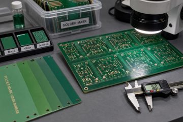
PCB Solder Mask: Purpose, Colors, Openings and DFM Checks
Learn what PCB solder mask does, how solder mask openings, colors, clearance, thickness and DFM checks affect fabrication, assembly and reliability.



Learn what PCB solder mask does, how solder mask openings, colors, clearance, thickness and DFM checks affect fabrication, assembly and reliability.
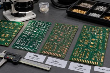
Compare PCB surface finish types including HASL, lead-free HASL, ENIG, OSP, immersion silver and immersion tin, with solderability, cost and DFM checks.
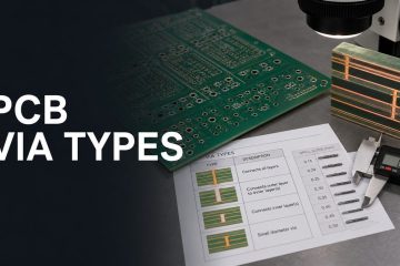
Learn the main PCB via types, how through vias, blind vias, buried vias, microvias and via-in-pad differ, and what to check before fabrication.
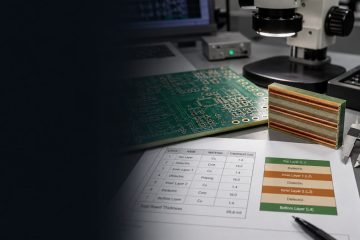
Learn a practical 4 layer PCB stackup, when to use signal-ground-power-signal layers, what to check for impedance, copper balance, vias and fabrication.
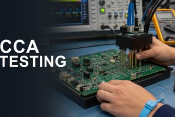
Learn circuit card assembly testing methods, what AOI, X-ray, ICT, flying probe and FCT can catch, what they miss, and what files to send before PCBA production.
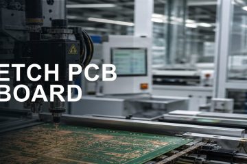
Learn how to etch a PCB board safely, from copper cleaning and resist transfer to etching checks, common failures and when to use factory fabrication.
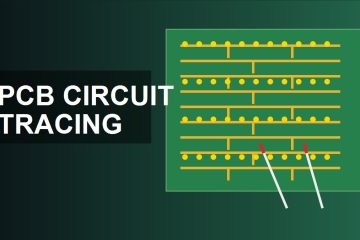
Learn how to trace a PCB circuit by following visible tracks, using continuity mode correctly, marking nets, checking components and preparing repair or remake notes.
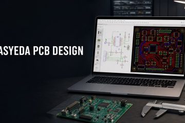
Learn how to use EasyEDA for PCB design from schematic and footprint checks through layout, DRC, Gerber export and manufacturing review.
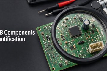
Use this PCB components identification chart to read reference designators, package clues, top markings, polarity and Pin 1, then confirm parts correctly.
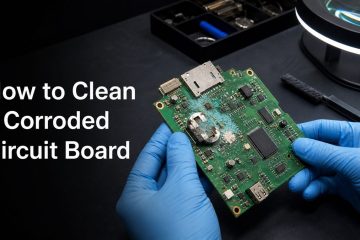
Learn how to identify the residue, clean a corroded circuit board safely, inspect damaged traces and pads, and test it before controlled power-up.
If you have any enquiry about quotation or cooperation, please feel free to email us at [email protected] or use the following enquiry form. Oursales representative will contact you within 24 hours. Thank you for your interest in our products.