Blog
Semi-Additive Process vs Subtractive Etching: PCB Fabrication DFM Differences
Compare semi-additive and subtractive PCB circuit formation through DFM: copper profile, imaging, plating, flash etch, inspection and supplier capability questions.




Compare semi-additive and subtractive PCB circuit formation through DFM: copper profile, imaging, plating, flash etch, inspection and supplier capability questions.
Decide when to keep using an evaluation board, choose a module and carrier, or start a custom PCB using product requirements and validation evidence.
Compare PCB vibration and mechanical shock testing, failure modes, fixtures, monitoring and test-plan choices. Also clarify why electrical shock is different.
Compare hot-swap and soldered keyboard PCBs by switch replacement, layout flexibility, repair, failure risks and manufacturing needs to choose the right board.
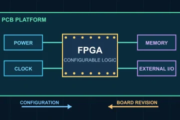
FPGA vs PCB explained: compare their functions, design files, costs and failure risks, then decide between a development board and a custom FPGA PCB.
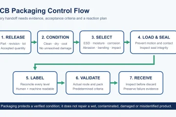
Control PCB packaging from clean-and-dry release through ESD and moisture protection, cushioning, labels, transport validation and receiving checks.
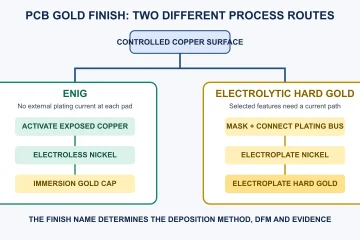
See how ENIG and electrolytic hard gold PCB processes differ, from pretreatment and nickel deposition to gold plating, inspection and RFQ controls.
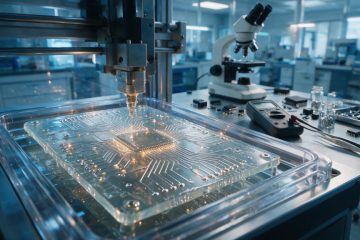
Yes, some 3D-printed circuits work—but a lit LED is not enough. Compare the processes, failure modes and tests that prove a prototype is usable.
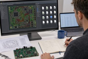
Learn how to identify and open PCB files safely, choose the right CAD or Gerber viewer, and verify layers, drills, units and revisions before manufacture.
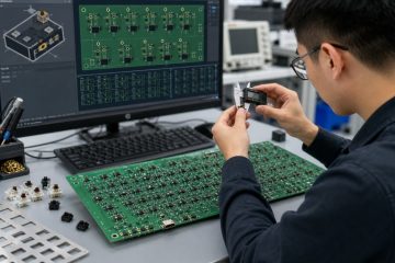
Design a hot-swappable keyboard PCB with compatible sockets, verified footprints, insertion support, matrix controls and full-key assembly testing.
If you have any enquiry about quotation or cooperation, please feel free to email us at [email protected] or use the following enquiry form. Oursales representative will contact you within 24 hours. Thank you for your interest in our products.