
Blog
PCB Blind Via Fabrication Process: Drilling, Plating and DFM Checks
See how PCB blind vias are planned, drilled, desmeared, plated and tested—and what stack-up, DFM and supplier evidence to verify before production.




See how PCB blind vias are planned, drilled, desmeared, plated and tested—and what stack-up, DFM and supplier evidence to verify before production.

See how the mSAP PCB process builds fine copper features, where plating and flash etching fail, and what DFM files and inspection evidence to request.
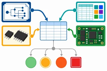
Cross-check a PCB schematic against the physical board, BOM, datasheets, and bounded measurements using an evidence map, mismatch classes, and clear stop conditions.
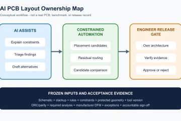
Evaluate AI for PCB layout by task scope, explicit constraints, verification gates, candidate evidence, IP controls, and accountable engineering sign-off.
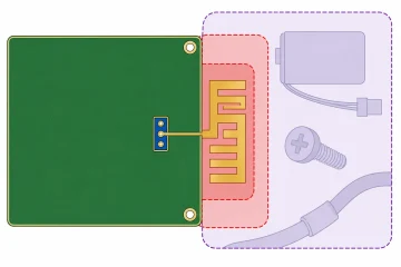
Design a 433 MHz PCB antenna layout with defensible geometry, ground and clearance rules, matching footprints, VNA tuning, enclosure checks and release evidence.

Learn how heavy copper PCBs are checked for copper geometry, plated-hole integrity, resistance, current capacity, temperature rise and reliability.
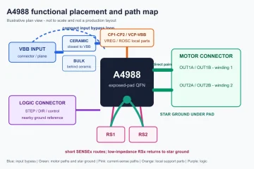
Design an A4988 PCB layout with datasheet-grounded placement, current-loop routing, sense paths, grounding, thermal vias, and bring-up checks.
Design a reliable 5V power supply PCB layout by classifying the rail, mapping buck current loops, routing feedback, reviewing USB boundaries, thermal paths and validation evidence.

See how HDI PCBs are built through laser microvias and sequential lamination, what can fail, and which test evidence to request before ordering.

See how rigid-flex PCBs are built, which process controls prevent transition and plating failures, and what test evidence to request before ordering.
If you have any enquiry about quotation or cooperation, please feel free to email us at [email protected] or use the following enquiry form. Oursales representative will contact you within 24 hours. Thank you for your interest in our products.