Blog
How to Make PCB Vias: Drill Data, Plating and DFM Checks
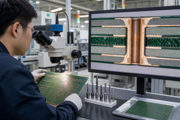
Learn how PCB vias are designed, drilled, desmeared and copper plated, how via treatments differ, and which DFM files and inspection checks prove quality.




Learn how PCB vias are designed, drilled, desmeared and copper plated, how via treatments differ, and which DFM files and inspection checks prove quality.
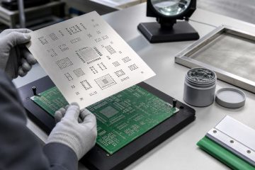
Make or order a PCB solder-paste stencil from the correct paste layers, review apertures and thickness, align it accurately, and approve the first print.
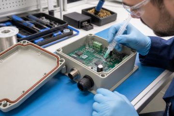
Waterproof a PCB by matching conformal coating, potting and enclosure sealing to the real exposure, then verify coverage, heat flow and product-level water tests.
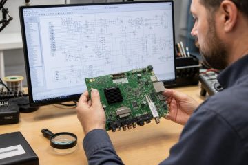
Find PCB schematics by board number and revision, check manufacturer and regulatory sources, trace missing circuits safely, and verify every document against the board.
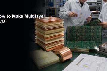
See how multilayer PCBs are designed, imaged, laminated, drilled, plated, finished, and tested, plus the files and DFM checks needed before fabrication.
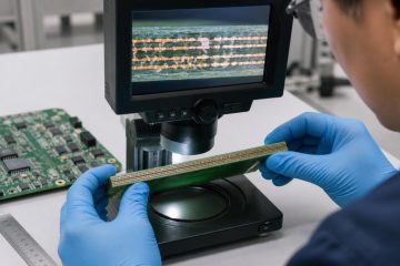
Learn how to identify PCB copper layers using design files, board-edge clues, vias, X-ray, and cross-section evidence, with clear limits for each method.

Evaluate a China PCB design service by defining inputs, stackup, DFM, review milestones, source-file ownership, and the final manufacturing handoff.
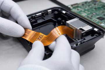
Learn how to make a flexible PCB by choosing the right stackup, protecting bend areas, preparing fabrication files, and checking the finished flex circuit.
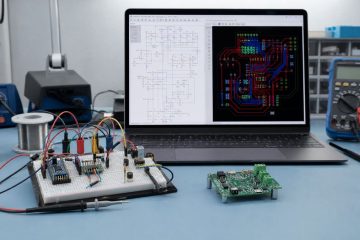
Convert a working breadboard into a manufacturable PCB using verified nets, footprints, layout rules, release files and a controlled first-board bring-up.
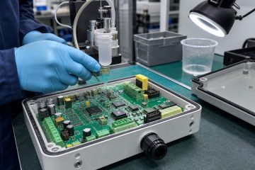
Learn how to protect a PCB from moisture using conformal coating, potting and enclosure sealing, then validate coverage, cure and product-level protection.
If you have any enquiry about quotation or cooperation, please feel free to email us at [email protected] or use the following enquiry form. Oursales representative will contact you within 24 hours. Thank you for your interest in our products.