




How is a multilayer PCB made?
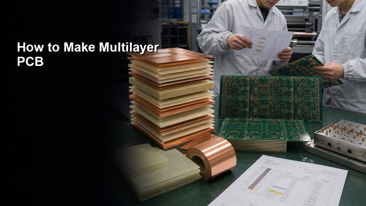
A multilayer PCB is made by imaging and etching inner copper layers, inspecting them, stacking cores and prepreg in a controlled order, laminating the stack under heat and pressure, drilling the cured panel, forming conductive hole walls, imaging the outer layers, applying finishes and solder mask, profiling the boards, and completing electrical and quality tests. Reliable production begins with an agreed stackup and fabrication package; the factory process cannot repair an electrically wrong layer plan.
Decide why the design needs more than two copper layers
Add layers to solve specific routing, reference-plane, power-distribution, EMC, isolation, density, or mechanical problems. A four-layer board may provide a continuous ground reference and more routing freedom, while six or more layers may help dense escape routing or separate critical functions. More layers also add fabrication operations, stackup constraints, cost, and failure opportunities.
| Design pressure | What another layer may provide | Question before adding it |
|---|---|---|
| Dense routing | Additional signal channels | Can placement or pin assignment reduce congestion? |
| Fast signals | Closer continuous reference planes | Is the return path controlled through every transition? |
| Power delivery | Low-inductance plane structures | Are current, copper, dielectric, and decoupling defined? |
| EMC risk | Better field containment | Are edges, connectors, gaps, and layer changes reviewed? |
| Mixed functions | Routing and reference separation | Does the split preserve return continuity? |
Build the stackup with the intended fabricator
The stackup defines copper layers, cores, prepreg, copper weight, dielectric thickness, finished thickness, material family, and sometimes impedance structures. Ask the intended fabricator for a build that meets electrical and mechanical needs using qualified materials and stable processes. Do this before critical routing; changing dielectric thickness later changes trace geometry and may alter via aspect ratio, press behavior, and finished thickness.
Assign a clear purpose to every copper layer
Name each layer by function: signal, ground reference, power distribution, mixed plane, or a controlled combination. Place critical signal layers next to continuous reference planes. Keep paired structures reasonably symmetric around the board center to reduce warpage risk. Avoid a stackup that forces high-speed traces to cross plane gaps or changes their reference without a return path.
Set fabrication rules before layout
Load trace width, spacing, via diameter, finished hole, annular ring, copper-to-edge, solder-mask, drill, and special-structure limits from the chosen process. For blind, buried, laser-drilled, filled, capped, controlled-depth, backdrilled, heavy-copper, flex, or sequential-lamination features, request a specific feasibility review. Do not infer these limits from a generic CAD preset.
Prepare inner-layer artwork and inspection data
Each inner copper layer is imaged on copper-clad core material and chemically etched. The factory then strips the resist and inspects the pattern, often using automated optical inspection against the CAM data. Inner defects must be found before lamination because they become inaccessible. Copper balancing, registration targets, coupons, and process compensation are handled during engineering and CAM preparation.
Treat and stack the inner layers
After inspection, inner copper surfaces receive the qualified bonding treatment. Operators or automated equipment arrange etched cores, prepreg sheets, and outer copper foil according to the traveler and stackup. Tooling and registration systems align the layers. Material identity, orientation, lot control, cleanliness, and foreign-material prevention matter at this stage.
Laminate the multilayer panel
The layup enters a press cycle where controlled heat, pressure, vacuum, and time allow prepreg resin to flow, fill, bond, and cure. The exact cycle belongs to the material and factory process. Poor registration, contamination, incorrect resin flow, trapped air, or an unsuitable construction can produce delamination, voids, thickness variation, or warpage.
Drill the laminated panel and remove drill residue
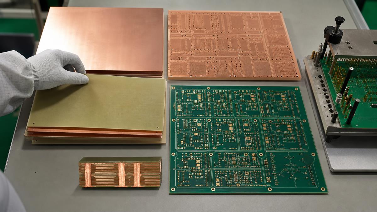
After lamination, the panel is registered and drilled for through holes and applicable via structures. Drilling exposes copper lands on internal layers. Heat and mechanical action can smear resin over the exposed copper, so the qualified cleaning and desmear process prepares the hole wall for metallization. Drill parameters, material, stack height, tool wear, hole size, and aspect ratio influence hole quality.
Create conductive hole walls
A thin conductive seed layer is formed on the nonconductive hole wall, followed by copper deposition or electroplating to build the required conductor. This connects the outer copper to the intended internal pads. The factory controls coverage, thickness, adhesion, and plating distribution. Cross-section coupons may be used to examine hole-wall copper, internal connections, and related quality features.
Image and plate the outer-layer pattern
The outer circuit pattern is imaged after drilling and initial hole metallization. Pattern plating builds copper on traces, pads, and hole walls as required by the process. The remaining unwanted outer copper is etched away. Because the outer layers have already passed through drilling and plating steps, their process sequence differs from the inner layers.
Apply solder mask, finish, legend, and profile
The panel is cleaned, coated with solder mask, imaged, developed, and cured. Exposed pads receive the specified surface finish. Legend is added where required, and the boards are routed, scored, or otherwise profiled from the production panel. Requirements for edge plating, castellations, countersinks, controlled depth, tight slots, or special finishes must be defined in the fabrication drawing.
Run electrical and quality checks
| Check | What it addresses | Evidence to request when critical |
|---|---|---|
| Electrical test | Opens and shorts against the net data | Test method and result by lot |
| AOI | Pattern defects on accessible process layers | Process record or exception disposition |
| Microsection | Layer registration, hole wall, interconnect, dielectric | Scaled coupon image and measurements |
| Impedance coupon | Controlled transmission structures | Coupon result tied to stackup and lot |
| Dimensional inspection | Outline, holes, thickness, tolerances | Inspection report where specified |
| Visual inspection | Finish, mask, marking, damage, workmanship | Agreed acceptance criteria |
Release a complete manufacturing package
- Gerber or ODB++ copper, mask, legend, profile, and applicable special layers
- NC drill and route data with tool and plated/non-plated distinction
- Fabrication drawing with stackup, finished thickness, copper, material, finish, and tolerances
- Controlled-impedance requirements and referenced coupons where applicable
- Via structure, hole span, fill, cap, backdrill, or sequential-build requirements
- IPC-356 or another approved netlist reference for electrical test
- Panel, marking, serialization, coupon, inspection, and certificate requirements
- Revision identity consistent across every file
Inspect the released data in an independent viewer. Confirm layer order, polarity, drills, outline, cutouts, and special notes before sending it.
Run a multilayer DFM review before ordering
Ask the fabricator to confirm stackup availability, impedance geometry, copper balance, resin and dielectric selection, registration allowance, via aspect ratio, annular rings, drill-to-copper clearances, special via sequence, panel support, finished thickness, tolerances, and test coupons. Resolve discrepancies in controlled files rather than leaving the final decision in informal messages.
Understand why DIY multilayer boards are hard to validate
A home experiment may align and bond multiple patterned sheets, but a production-quality board also needs controlled materials, registration, resin flow, hole-wall preparation, plated interconnects, inspection, and electrical verification. Hand-added wires or rivets are not equivalent to qualified plated through holes, and a board that powers on does not prove long-term interconnect reliability. For a learning experiment, keep voltage and risk low and label the construction as experimental. For a product, use professional fabrication.
Avoid common multilayer PCB mistakes
- Routing before the stackup is approved
- Adding layers without assigning clear functions
- Breaking return paths with plane gaps or careless layer changes
- Using unsupported via types or aspect ratios
- Ignoring copper balance and board symmetry
- Sending ambiguous layer names or inconsistent revisions
- Omitting netlist, impedance, coupon, or special inspection requirements
- Approving production without viewing final fabrication data
Multilayer PCB FAQ
What is the minimum number of layers in a multilayer PCB?
The term generally refers to a board with internal copper layers in addition to the outer copper. Common commercial constructions start at four copper layers, although terminology and special constructions should be confirmed with the fabricator.
Can I make a four-layer PCB at home?
You can experiment with stacked conductors, but controlled registration, lamination, plated holes, material behavior, and verification make a reliable production-equivalent four-layer board impractical for most home workshops.
Why is prepreg used?
Prepreg is resin-impregnated reinforcement that bonds layers and becomes part of the dielectric structure during lamination. Its cured thickness and resin behavior affect the final stackup.
When are inner layers etched?
Inner copper patterns are imaged, etched, stripped, and inspected before the layers are stacked and laminated.
How do vias connect internal layers?
Drilling exposes internal copper pads; qualified hole preparation and metallization create conductive walls that connect the specified copper layers.
Why is desmear important?
It removes or modifies resin residue left on exposed internal copper after drilling so the subsequent metallization can form a reliable electrical connection.
How do I choose four versus six layers?
Choose based on routing density, reference planes, power distribution, signal integrity, EMC, mechanics, and cost. Review a proposed stackup rather than choosing only by component count.
What files does a multilayer PCB manufacturer need?
Provide fabrication artwork, drill/route data, stackup and drawing, material and finish requirements, special via definitions, netlist, impedance requirements, tolerances, quantity, and controlled revision information.
How is a multilayer PCB tested?
Electrical testing checks continuity and isolation. Process and quality verification may also include AOI, microsections, impedance coupons, dimensions, visual inspection, and other project-specific tests.
Does a higher layer count always improve the design?
No. Extra layers help only when their functions and references solve real design constraints. Unnecessary layers increase cost and manufacturing complexity.
Request stackup and multilayer DFM review
Send your fabrication data, proposed layer functions, thickness, material needs, impedance targets, via structures, quantity, and inspection requirements through the PCBTRY contact page. Request a stackup and DFM review before critical routing or production release.



1 Comment
Semi-Additive Process vs Subtractive Etching: PCB Fabrication DFM Differences - thindry pcb manufacturer · 08/26/2026 at 08:34
[…] Fine routing is one part of a board. Stackup construction, dielectric thickness, via sequence, plating requirements, surface finish, solder-mask registration and test access may become the actual release constraint. For a broader manufacturing-input review, see PCBtry’s guide to multilayer PCB stackup, lamination and DFM checks. […]