Blog
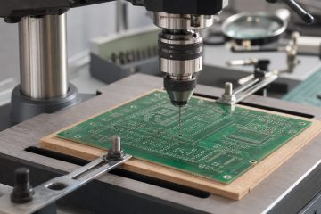
How to Drill a PCB: Bit Sizes, Setup and Hole Quality Checks
Learn how to choose PCB drill bits, set up the board, drill clean holes, inspect defects and prepare drill data for reliable PCB fabrication.



Learn how to choose PCB drill bits, set up the board, drill clean holes, inspect defects and prepare drill data for reliable PCB fabrication.
Learn how PCB etch factor changes finished trace width, impedance and fine-line DFM, with formulas, examples and fabrication checks.
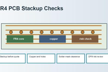
Understand how an FR4 printed circuit board is built, what to check in stackup and fabrication, and when standard FR4 needs review.
Learn how to etch a PCB board safely, from copper cleaning and resist transfer to etching checks, common failures and when to use factory fabrication.
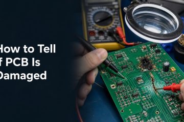
Learn how to tell if PCB is damaged by checking burn marks, broken traces, lifted pads, shorts, power rails, hot parts and repair or remake decisions.
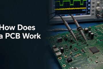
Learn how a PCB works through copper traces, layers, power paths, components, vias, ground planes, test points and manufacturing checks.
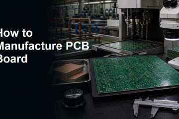
Learn how to manufacture PCB board from Gerber files through imaging, drilling, plating, solder mask, silkscreen, surface finish, inspection, and DFM checks.
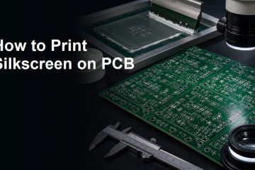
Learn how to print silkscreen on PCB with legend layers, pad clearance, useful markings, manufacturing limits, readability checks, and DFM review.
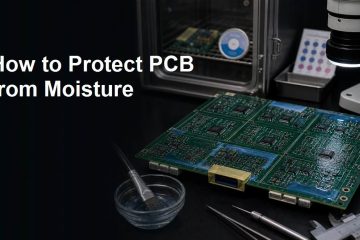
Learn how to protect PCB from moisture with design spacing, conformal coating, masking, cleaning, storage, inspection, and DFM review.
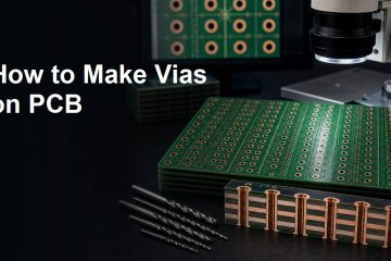
Learn how to make vias on PCB with drilling, copper plating, via types, annular ring checks, aspect ratio limits, and DFM notes before fabrication.
If you have any enquiry about quotation or cooperation, please feel free to email us at [email protected] or use the following enquiry form. Oursales representative will contact you within 24 hours. Thank you for your interest in our products.