Blog
How to Tell How Many Layers a PCB Has: Vias, Edges and Stackup Checks
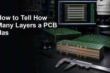
Learn how to tell how many layers a PCB has using edge inspection, vias, light checks, stackup clues, and when to ask a manufacturer for confirmation.



Learn how to tell how many layers a PCB has using edge inspection, vias, light checks, stackup clues, and when to ask a manufacturer for confirmation.
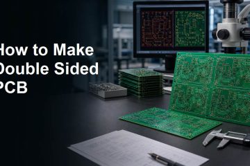
Learn how to make double sided PCB with copper layers, plated vias, alignment, DFM checks, Gerber files and manufacturing review.
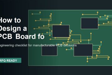
Learn how to design a PCB board for a circuit, from schematic and footprints to layout, DFM checks, manufacturing files and quote-ready review.
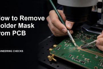
Learn how to remove solder mask from a PCB safely, including tools, step-by-step repair workflow, inspection checks, copper protection and supplier review notes.
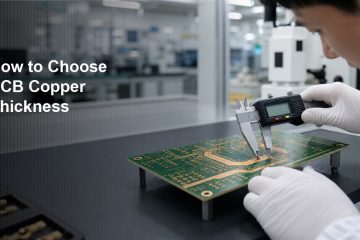
Learn how to choose PCB copper thickness by current load, trace width, temperature rise, via plating, layer stackup and manufacturing cost.
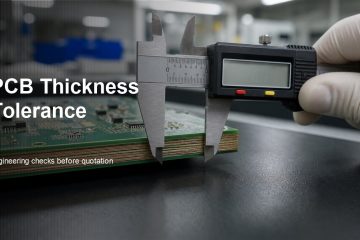
Learn what PCB thickness tolerance means, how finished board thickness is measured, and what buyers should confirm in stackup, copper, finish and RFQ notes.

Review aluminum PCB China sourcing by thermal path, dielectric, copper weight, finish, testing, and RFQ documentation.

Compare flexible PCB manufacturer China options by material, bend area, stiffener, testing, and RFQ checks before production.

Use this China PCB prototype service guide to prepare Gerber files, specs, DFM questions, quote checks, and first-batch decisions.
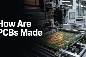
Learn how PCBs are made in a factory, from Gerber review and layer imaging to etching, drilling, plating, solder mask, surface finish and electrical testing.
If you have any enquiry about quotation or cooperation, please feel free to email us at [email protected] or use the following enquiry form. Oursales representative will contact you within 24 hours. Thank you for your interest in our products.